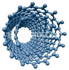
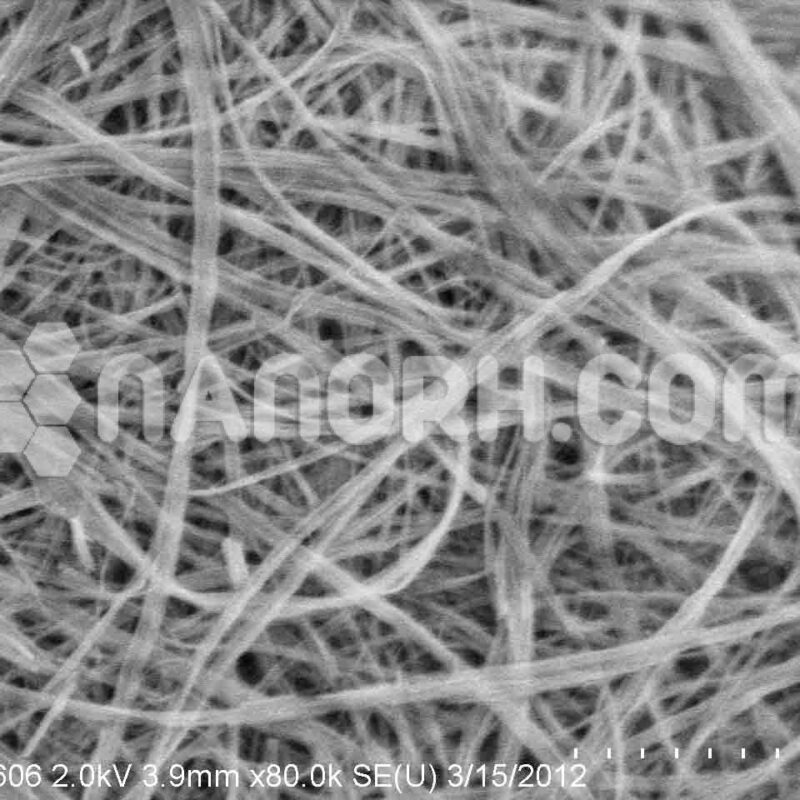
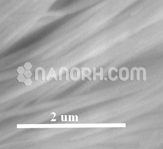
Silicon Dioxide Nanospheres
Chemical Vapor Deposition (CVD) and Physical Vapor Deposition (PVD) processes including Thermal and Electron Beam (E-Beam) Evaporation, Low Temperature Organic Evaporation, Atomic Layer Deposition (ALD), Metallic-Organic and Chemical Vapor Deposition (MOCVD). Our standard slug sizes range from 1/8″ x 1/8″ to 1/4″ x 1/4″ and 3 mm diameter. We can also provide spheres outside this range for ultra high purity thin film applications, such as fuel cells and solar energy layers. Materials are produced using crystallization..
| Silicon Dioxide Nanospheres | |
| Product No | NRE-15006 |
| CAS No. | 60676-86-0 |
| Formula | SiO2 |
| Average diameter | 30-50nm |
| Purity | 99.9% |
| Molecular Weight | 60.09 g/mol |
| Density | 2533 kg/m-3 |
| Melting Point | 1,600° C |
| Boiling Point | 2,230° C |
Silicon Dioxide Nanospheres
Elements specialize in producing purity uniform Silicon Dioxide Nanospheres with the highest possible density and smallest possible average grain sizes for use in semiconductor, Chemical Vapor Deposition (CVD), and Physical Vapor Deposition (PVD) processes including Thermal and Electron Beam (E-Beam) Evaporation, Low-Temperature Organic Evaporation, Atomic Layer Deposition (ALD), Metallic-Organic and Chemical Vapor Deposition (MOCVD). Our standard slug sizes range from 1/8″ x 1/8″ to 1/4″ x 1/4″ and 3 mm in diameter. We can also provide spheres outside this range for ultra-high purity thin film applications, such as fuel cells and solar energy layers. Materials are produced using crystallization, solid-state, and other ultra-high purification processes such as sublimation. Elements specializes in producing custom compositions for commercial and research applications and for new proprietary technologies. Elements also cast any of the rare earth metals and most other advanced materials into rod, bar, or plate form, as well as other machined shapes and through other processes such as nanoparticles and in the form of solutions and organometallics. We also produce Silicon Dioxide as pieces, tablets, powder, and sputtering targets. Oxide compounds are not conductive to electricity. However, certain perovskite structured oxides are electronically conductive finding applications in the cathode of solid oxide fuel cells and oxygen generation systems. Other shapes are available by request. Silicon for solar energy applications includes p-type and n-type silicon thin film layers which can be fabricated by deposition utilizing AE Solar Energy silicon. Silicon-based photovoltaic cells (PV Cells) for solar energy are fabricated from a positively charged or p-type silicon layer underneath a negatively charged or n-type silicon layer. See Safety information.