Silicon Wafers
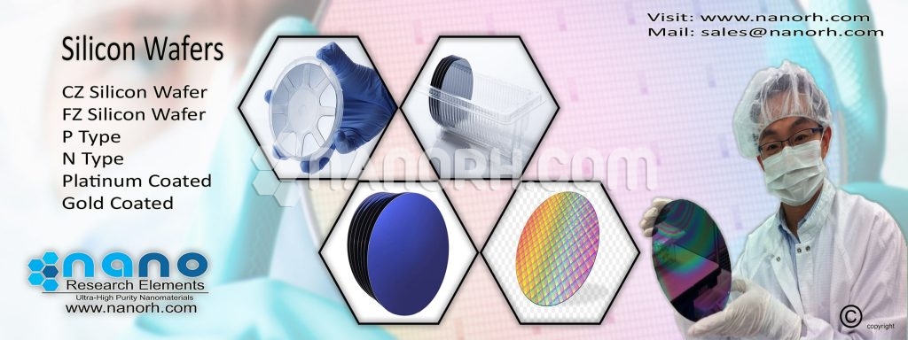
SILICON WAFERS
Introduction
Silicon is the second most common element on Earth and is the seventh most common element in the entire universe. It is the most common semiconductor and the most widely used in the electronic and technological sector. There are several silicon wafers fabrication methods, including the horizontal gradient freezing method, the horizontal Bridgeman method, the vertical Bridgeman method, the vertical gradient freezing and, finally, the Czochralski drag method.
During the silicon wafers growth process to obtain the derived purity, several intentional dopants are added. These introduced impurities can modify the electrical properties of silicon wafers, which can be useful depending on what silicon wafers eventually produces. Boron, aluminum, nitrogen, gallium, and indium are just some of the silicone dopants that can be introduced during the growth process. Depending on the level at which the silicon wafers have been doped, the semiconductor can be considered extrinsic or degenerate. The extrinsic must be slightly doped while the degenerate semiconductors act more as conductors due to the high levels of dopant that are produced during manufacturing. Silicon wafers are a key component in integrated circuits. Integrated circuits are, in short, a composite of several electronic components arranged to perform a specific function. Silicon wafers are the main platform for semiconductor devices. A silicon wafer is a thin slice of this semiconductor material, which acts as a substrate for microelectronic devices embedded in the wafer.
Types of silicon wafers substrates
Semiconductors of a single element
Silicon, Si is the most common semiconductor with atomic number 14, energy gap, for example, = 1.12 eV, indirect band gap; Crystal-diamond structure, constant lattice -0.543 nm, thermal conductivity 1.31 W / cm-oC, melting point 1414 ° C thanks to these crystal properties it is possible to work on silicon wafers up to 300 mm in diameter and with excellent mechanical properties in applications MEMS.
Silicon on Insulator (SOI)
Only a thin layer is used on the surface of a silicon wafer to make electronic components; The rest essentially serves as mechanical support. The role of SOI is to electronically isolate a thin layer of monocrystalline silicon from the rest of the silicon wafers. Integrated circuits can be produced in the top layer of SOI wafers using the same processes that would be used in simple silicon wafers. The integrated insulation layer allows SOI-based chips to operate at significantly higher speeds while reducing electrical losses. The result is an increase in performance and a reduction in energy consumption. There are two types of SOI wafers. Thin-film SOI wafers have a device layer <1.5 m and film wafers often have a device layer> 1.5 m. The union of silicon wafers. - In this process, the surface of two wafers is covered by an insulating layer (usually oxide). The insulating layers are then bonded in an oven, creating a single wafer with a layer of buried oxide (CAJA) inserted between layers of semiconductors. The upper part of the wafer overlaps and shines until it reaches the desired thickness of the semiconductor above the BOX. SIMOX - Separation for rust plant. In this process, a mass semiconductor silicon wafers is bombarded with oxygen ions, creating a layer of buried oxide. The thickness of the intrinsic semiconductor on the box is determined by the energy of the ions. Annealing strengthens the Si-O bonds in the box. Intelligent cutting: the silicon wafers bonding method is used to form the BOX, but instead of licking the excess semiconductor (which is a waste), a hydrogen layer is implanted at a depth that specifies the desired active semiconductor layer. Annealing at ~ 500 oC divides the silicon wafers along the plane of tension created by the implanted hydrogen. The divided wafer can be reused to form other SIO wafers.
III-V Semiconductors
Gallium arsenide (GaAs): after the second silicon, the most common semiconductor is GaAs with energy space, for example, = 1.43 eV, direct band space; Crystal structure: zinc mixture, thermal conductivity 0.46 W / cm-oC, thermally unstable above 600 oC. Due to the evaporation, they do not form native oxide of sufficient quality and mechanically fragile. Due to the bandwidth commonly used to make devices that emit light. Due to the greater mobility of electrons and holes, use for the variety of high-speed electronic devices. The space between bands can be easily designed by forming ternary compounds based on GaAs, p. Eg AlGaAs. Gallium Nitride (GaN): broadband of III-V semiconductor with a direct bandwidth of 3.5 eV wide; Among very few semiconductors capable of generating blue radiation. GaN is used for LED and blue laser; An intrinsic n-type semiconductor, but it can be p-doped. GaN is formed as an epitaxial layer. The lattice misalignment is still a problem, creating a high density of defects. The incorporation of Indio (InxGa1-xN) allows the control of emissions from green to violet (maximum and minimum content, respectively). GaN can also be used in UV detectors that do not respond to visible light. GaN has a crystal structure Wurtzite (W) or Zinc Blend (ZB)
Other binary semiconductors
Silicon carbide (SiC): the semiconductor with energy gap, for example, = 2.9 -3.05 eV (broadband semiconductor), indirect band gap; SiC can be obtained in different polyposes, the most common hexagon in the form of 4H or 6H polytypes; The parameters vary according to the politipo. Doped inherently with n; P-type doping and n-type conductivity control can be obtained by doping respectively with aluminum and nitrogen. The SiC characteristics are higher than the electronic saturation rate of Si and GaAs; Excellent semiconductor, but difficult and expensive to manufacture monocrystalline wafers; Excellent for high power and high temperature applications; SiC is strictly reticular adapted to GaN, has a coefficient of thermal expansion close to GaN and is available in both conductive and semi-insulating substrates. Therefore, it is often used as a substrate for the epitaxial layers of GaN. The 75 mm diameter SiC wafers are commercially available.
Fiber Optic
Silicon is the cheapest IR material available. Both P-type and N-type substrates are acceptable for IR optics as long as they offer a transmission greater than 50% at a wavelength between 1.5 and 6 microns. In general terms, for type N, the resistivity must be greater than 20 ohm-cm and, for type P, greater than 40 ohm-cm. For use in the near IR, this is not so important, but for applications for far IR, the resistivity can be critical. Float Zone Silicon meets the criteria for optical use.
Uses of silicon wafers
The main use of silicon wafers is in integrated circuits. Integrated circuits feed many of the devices that modern society uses every day. Computers and smartphones are just two of the devices that depend on this technology. Although the other semiconductors have been tested overtime, silicon wafers has proven to be a stable option. Other uses include sensors, such as the tire pressure sensor system and solar cells. Silicon slices absorb photons from sunlight and this in turn generates electricity. Silicon wafers are also used for various nanomaterial coating applications such as biosensitivity.