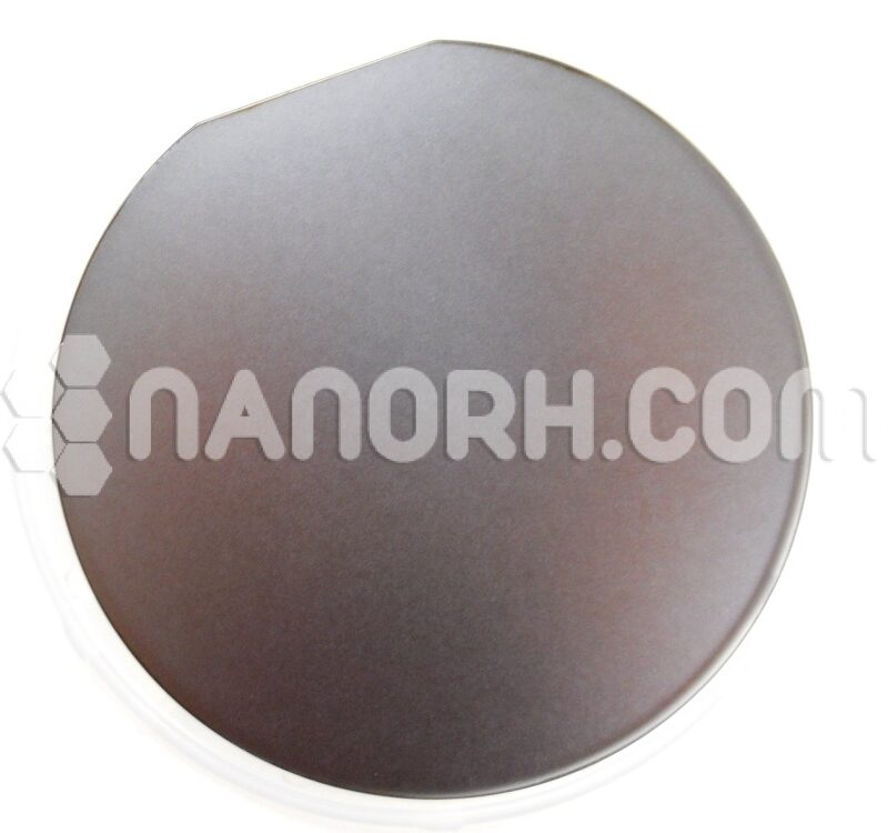
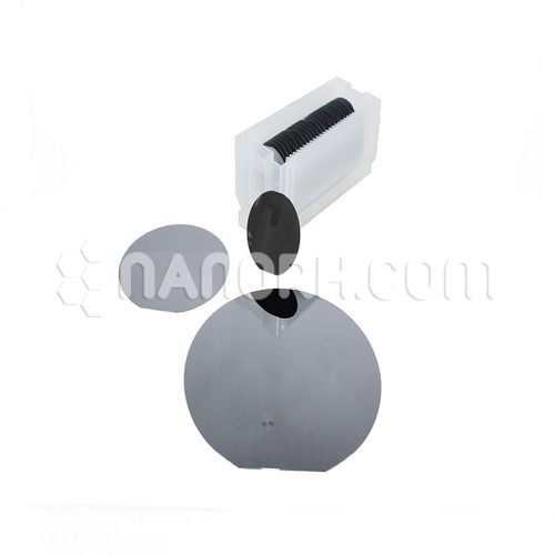
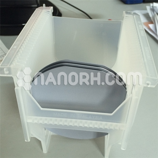
3 inch silicon wafer N Type
| 3 inch silicon wafer N Type | |
| Product No | NRE-44001 |
| Type | N-Type |
| Formula | Si |
| Crystal method | CZ |
| Purity | NA |
| Thickness | 250-500μm |
| Diameter (mm) | 3” (76.2mm) |
| Doping | Phosphorous |
| Resistivity | 1-10ohm-cm |
| RRG (%) | ≤12 |
3 inch silicon wafer N Type
Introduction:
3 inch Silicon wafer N type are fundamental substrates in the semiconductor industry, serving as the foundation for fabricating electronic devices. A 3-inch (75 mm) silicon wafer is a common size used for various applications, especially in research and development and smaller-scale manufacturing. N-type silicon wafers are doped with elements like phosphorus or arsenic, which provide excess electrons, enhancing their electrical conductivity.
Properties
Doping Elements: Typically doped with phosphorus (P) or arsenic (As), which donate free electrons to the silicon lattice.
Electrical Conductivity: N-type silicon exhibits higher electron concentration, making it suitable for various electronic components.
Crystal Structure: Usually produced in single crystal form (Czochralski or Float Zone methods), ensuring uniformity and high purity.
Applications
Integrated Circuits (ICs): Used in the fabrication of microprocessors, memory chips, and other semiconductor devices.
Solar Cells: N-type wafers can be used in photovoltaic cells for improved efficiency and performance.
Sensors: Employed in various sensor technologies, including temperature sensors and pressure sensors.
Transistors: Forming the basis for bipolar junction transistors (BJTs) and field-effect transistors (FETs).
Research and Development: Commonly used in laboratories for experiments and prototyping new semiconductor devices.