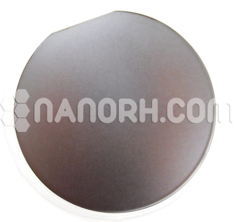
Boron Doped Silicon Wafer
| Boron Doped Silicon Wafer | |
| Product No | NRE-44004 |
| Type | P-type |
| Formula | B-Si |
| Crystal method | CZ |
| Purity | NA |
| Thickness | 250-500μm |
| Diameter (mm) | 2” (50.8mm) |
| Doping | Boron |
| Resistivity | 1-10ohm-cm |
| RRG (%) | ≤12 |
| Oxygen Contents (ppma) | 12.5-16.5 |
Boron Doped Silicon Wafer
Introduction:
Boron doped silicon wafer are a crucial component in the semiconductor industry. Doping silicon with boron, a trivalent element, creates P-type silicon, which has an abundance of holes (positive charge carriers). This alteration in the electrical properties of silicon makes it suitable for a wide range of applications in electronic and optoelectronic devices.
Properties
Doping Mechanism: Boron atoms replace some silicon atoms in the crystal lattice, creating “holes” that allow for electrical conduction.
P-Type Conductivity: Characterized by higher hole concentration, which facilitates positive charge flow.
Crystal Structure: Typically produced as single crystal wafers, ensuring uniformity and high purity.
Applications
Integrated Circuits (ICs): Used in the fabrication of microprocessors, memory chips, and analog devices, forming the basis for various electronic functionalities.
Solar Cells: Essential for photovoltaic technologies, particularly in creating p-n junctions when combined with N-type silicon, which enhances light absorption and energy conversion.
Transistors: Commonly used in bipolar junction transistors (BJTs), which amplify signals and switch electronic currents.
Diodes: Found in various types of diodes, including rectifiers and light-emitting diodes (LEDs), utilizing their p-n junction properties for efficient operation.
Sensors: Integral to the development of various sensors, including temperature sensors, pressure sensors, and gas sensors.
MEMS Devices: Employed in microelectromechanical systems, which are used for applications ranging from automotive to consumer electronics.