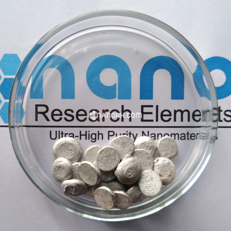
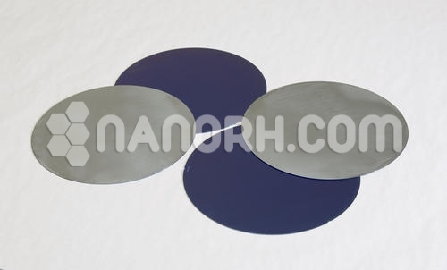
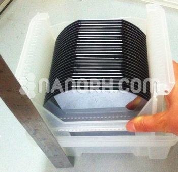
Arsenic Telluride Sputtering Targets
Arsenic Telluride Sputtering Targets
| Arsenic Telluride Sputtering Targets | |
| Product No | NRE-43324 |
| CAS No. | 12044-54-1 |
| Formula | As2Te3 |
| Molecular Weight | 532.64 |
| Purity | >99.9% |
| Density | NA |
| Thickness | 3 mm ± 0.5mm (can be customized) |
| Diameter | 50 mm ± 1mm (can be customized) |
| Shape | Round |
| Resistivity | NA |
| Thermal Conductivity | NA |
Arsenic Telluride Sputtering Targets
Arsenic telluride (As_2Te_3) sputtering targets are used in various applications, particularly in the production of thin films for electronic and optoelectronic devices.
Photovoltaics
Arsenic telluride is used in the manufacturing of thin-film solar cells. The material is part of the semiconductor layer in these cells, which helps in converting sunlight into electricity efficiently.
Optoelectronics
Arsenic telluride thin films are used in optoelectronic devices such as infrared detectors and sensors. These devices can detect infrared radiation and are used in applications like thermal imaging and night vision.
Semiconductor Devices
In some specialized semiconductor devices, arsenic telluride is used for its unique electronic properties. It can be part of the active layers in devices such as photodetectors and switches.
Thermoelectric Materials
Arsenic telluride can be used in thermoelectric materials, which convert temperature differences into electrical voltage. These materials are useful in power generation and cooling applications.
Material Research and Development
Researchers use arsenic telluride sputtering targets to explore new materials and processes in thin-film technology. The precise control over film thickness and composition provided by sputtering is valuable for developing new semiconductor materials and devices.
Sputtering Process Overview:
Sputtering involves bombarding the target material (arsenic telluride in this case) with high-energy particles, which eject atoms from the target. These atoms then deposit onto a substrate, forming a thin film.
This process is performed in a vacuum chamber, and various parameters such as temperature, pressure, and sputtering power can be adjusted to achieve the desired film properties.