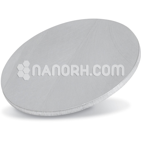
| Gallium Selenide Sputtering Targets | |
| Product No | NRE-43422 |
| CAS No. | 12024-24-7 |
| Formula | Ga2Se3 |
| Molecular Weight | 376.33 g/mol |
| Purity | >99.9% |
| Density | 4.92 g/cm3 |
| Thickness | 3 mm ± 0.5mm (can be customized) |
| Diameter | 50 mm ± 1mm (can be customized) |
| Shape | Round |
| Resistivity | NA |
| Thermal Conductivity | NA |
Gallium Selenide Sputtering Targets
Gallium selenide (GaSe) sputtering targets are used in various applications due to their unique properties as a semiconductor material. Here are some key application..
Photovoltaics
Solar Cells: GaSe can be used in thin-film solar cells, where it serves as a light-absorbing layer, contributing to the efficiency of energy conversion.
Optoelectronics
LEDs: GaSe is utilized in the fabrication of light-emitting diodes, particularly in the infrared and visible regions, due to its direct bandgap.
Laser Diodes: It can also be used in laser diode applications, providing efficient light emission.
Nonlinear Optics
Optical Devices: GaSe is employed in nonlinear optical devices for frequency doubling and other nonlinear processes, due to its high nonlinearity and good optical properties.
Photodetectors
Infrared Sensors: GaSe is used in photodetectors, especially for infrared detection applications, benefiting from its sensitivity to a wide range of wavelengths.
2D Materials Research
Layered Structures: GaSe is a member of the family of transition metal dichalcogenides (TMDs), making it relevant in research for developing new 2D materials for electronics and optoelectronics.
Thin Film Transistors (TFTs)
GaSe can be utilized in TFTs, enhancing electronic performance in displays and other electronic devices.


