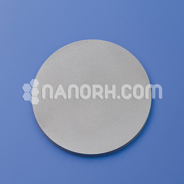
| GeAsSe Sputtering Targets | |
| Product No | NRE-43428 |
| CAS No. | NA |
| Formula | GeAsSe |
| Molecular Weight | NA |
| Purity | >99.9% |
| Density | NA |
| Thickness | 3 mm ± 0.5mm (can be customized) |
| Diameter | 50 mm ± 1mm (can be customized) |
| Shape | Round |
| Resistivity | NA |
| Thermal Conductivity | NA |
GeAsSe Sputtering Targets
Gallium arsenide selenide (GeAsSe) sputtering targets are used in various advanced applications, particularly in optoelectronics and materials science. Here are some key applications.
Optoelectronic Devices
Photodetectors: GeAsSe is utilized in photodetectors, particularly in the infrared range, making it suitable for applications in imaging and sensing technologies.
Light-Emitting Diodes (LEDs): This material can be employed in the fabrication of LEDs, especially for infrared and visible light emissions.
Chalcogenide Glasses
Data Storage: GeAsSe is a component in chalcogenide glasses used in phase-change memory technologies, benefiting from their ability to change states between amorphous and crystalline forms.
Solar Cells
Thin-Film Photovoltaics: GeAsSe can be utilized as a light-absorbing layer in thin-film solar cells, enhancing energy conversion efficiency.
Nonlinear Optical Applications
Frequency Conversion: The material’s nonlinear optical properties allow for its use in devices requiring frequency doubling and other nonlinear processes.
Thermal Imaging
Thermal Detectors: GeAsSe can be employed in thermal imaging applications due to its sensitivity to infrared radiation.
Research and Development
Materials Science: GeAsSe is of interest in the study of new materials for potential applications in photonics, electronics, and sensors.
Summary
GeAsSe sputtering targets are valuable for a range of applications, especially in optoelectronics and data storage technologies. Their unique properties enable advancements in various high-tech fields, making them a significant material for ongoing research and development.


