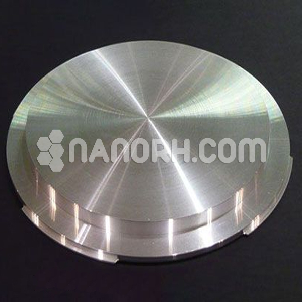
| Germanium Dioxide Sputtering Targets | |
| Product No | NRE-43431 |
| CAS No. | 1310-53-8 |
| Formula | GeO2 |
| Molecular Weight | 104.6388 g/mol |
| Purity | >99.9% |
| Density | 4.228 g/cm3 |
| Thickness | 3 mm ± 0.5mm (can be customized) |
| Diameter | 50 mm ± 1mm (can be customized) |
| Shape | Round |
| Resistivity | NA |
| Thermal Conductivity | NA |
Germanium Dioxide Sputtering Targets
Germanium dioxide (GeO₂) sputtering targets are utilized in various applications due to their unique properties as a semiconductor and insulator. Here are some key applications.
Optoelectronics
Optical Coatings: GeO₂ is used in optical coatings, providing high refractive index layers for lenses, mirrors, and other optical components.
Waveguides: Employed in the fabrication of optical waveguides for integrated photonics.
Thin Film Transistors (TFTs)
Electronics: GeO₂ can be used as a gate dielectric material in thin film transistors, improving performance in display technologies.
Sensors
Gas and Chemical Sensors: The material can be used in sensor applications, particularly for detecting gases and environmental monitoring.
Memory Devices
Non-Volatile Memory: GeO₂ is explored for use in phase-change memory and other non-volatile memory technologies, benefiting from its switching capabilities.
High-Performance Dielectrics
Capacitors and RF Devices: GeO₂ can serve as a dielectric material in capacitors, contributing to improved performance in radio frequency (RF) and microwave applications.
Research and Development
Material Studies: GeO₂ is of interest in materials science for the development of new semiconductors and advanced electronic materials.


