In2Sb3 Sputtering Targets
In2Sb3 Sputtering Targets
| In2Sb3 Sputtering Targets | |
| Product No | NRE-43444 |
| CAS No. | NA |
| Formula | In2Sb3 |
| Molecular Weight | NA |
| Purity | >99.9% |
| Density | NA |
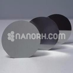
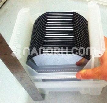
| Thickness | 3 mm ± 0.5mm (can be customized) |
| Diameter | 50 mm ± 1mm (can be customized) |
| Shape | Round |
| Resistivity | NA |
| Thermal Conductivity | NA |
In2Sb3 Sputtering Targets
Introduction
In₂Sb₃ (Indium Antimonide) sputtering targets are materials used in the deposition of indium antimonide thin films through sputtering techniques. In₂Sb₃ is a semiconductor compound known for its unique electrical and optical properties, particularly in infrared applications. Its characteristics make it suitable for a variety of advanced technological applications, especially in the fields of optoelectronics and infrared sensing.
Applications of In₂Sb₃ Sputtering Targets
Infrared Detectors:
In₂Sb₃ is widely used in the fabrication of infrared detectors and sensors, including those for thermal imaging and spectroscopy. Its sensitivity to infrared radiation makes it ideal for applications in military and industrial sectors.
Thermal Imaging Cameras:
The compound is used in thermal imaging devices, providing high-resolution images based on infrared radiation, which is crucial for applications such as surveillance, search and rescue, and firefighting.
Optoelectronic Devices:
In₂Sb₃ is employed in various optoelectronic devices, including light-emitting diodes (LEDs) and laser diodes, particularly for applications that require infrared light emission.
Semiconductor Applications:
As a semiconductor material, In₂Sb₃ can be utilized in electronic devices, including transistors and integrated circuits, particularly in specialized applications that require high sensitivity and low noise.
Research and Development:
In₂Sb₃ sputtering targets are valuable in material science research, enabling the exploration of new properties and functionalities in thin film technologies, particularly for emerging infrared and optoelectronic applications.
Thermoelectric Devices:
The material’s properties can also be leveraged in thermoelectric applications, where it is used for converting temperature differences into electrical voltage.
In summary, In₂Sb₃ sputtering targets are crucial for advancing technologies in infrared detection and optoelectronics, enabling the production of high-quality thin films that meet the demands of modern applications in various fields.