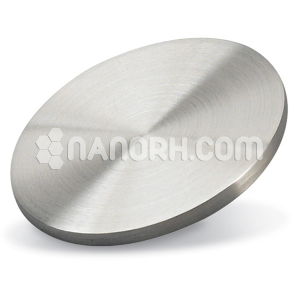
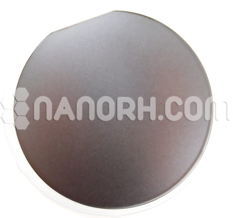
| Indium Arsenide Sputtering Targets | |
| Product No | NRE-43446 |
| CAS No. | 1303-11-3 |
| Formula | InAs |
| Molecular Weight | 189.74 |
| Purity | >99.9% |
| Density | 5.67 g/cm3 |
| Thickness | 3 mm ± 0.5mm (can be customized) |
| Diameter | 50 mm ± 1mm (can be customized) |
| Shape | Round |
| Resistivity | NA |
| Thermal Conductivity | NA |
Indium Arsenide Sputtering Targets
Indium arsenide (InAs) sputtering targets are primarily used in the fabrication of semiconductor devices, particularly in the production of high-speed electronics and optoelectronics. Here are some key applications.
Infrared Detectors: InAs is sensitive to infrared light, making it suitable for infrared sensor applications, such as thermal imaging and spectroscopy.
High Electron Mobility Transistors (HEMTs): InAs is used in the development of HEMTs, which are important for high-frequency and high-speed applications, including telecommunications.
Quantum Dots: InAs quantum dots are used in various optoelectronic applications, including lasers and photodetectors, due to their tunable bandgap properties.
Photovoltaic Cells: InAs can be used in multi-junction solar cells to improve efficiency by absorbing a wider range of the solar spectrum.
Nanoelectronics: The unique electronic properties of InAs make it a material of interest in the development of next-generation nanoelectronic devices.
Research and Development: InAs is often used in research settings to study semiconductor physics and to develop new materials and devices.
Sputtering is a preferred deposition technique for these applications due to its ability to create thin films with precise thickness control and uniformity.


