Indium Phosphide Nanoparticles
Indium Phosphide Nanoparticles
1) Indium Phosphide (InP) is an individual from the III-V group of semiconductors. III-V materials are paired molecules with one component from the metallic group 3 of the periodic table, and one from the non-metallic group 5. Some of these compounds are known for their high electrons and holes mobility, which on account of the best-known illustration – gallium arsenide – for very high-speed electronics.
2) III-V compounds have a cubic lattice type structure with atoms in each corner. Indium Phosphide, for instance, highlights interchange indium and phosphorous atoms. As a semiconductor, InP has an energy bandgap, which make it opaque for the light energy that is higher than the bandgap, and transparent for light energy levels that are below.
3) A group of materials – including InGaAs and InGaAsP – share an indistinguishable 5.87å cross section steady from InP, permitting epitaxial handling over the fundamental Indium Phosphide wafer.
| Indium Phosphide Nanoparticles | |
| Product No | NRE-5110 |
| CAS | 22398-80-7 |
| Purity | 99.9% |
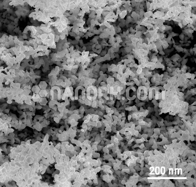
| APS | <100 nm (can be customized) |
| Formula | InP |
| Molecular Weight | 145.79g/mol |
| Density | 4.81g/cm3 |
| Color | Black |
| Melting Point | 1062°C |
| Boiling Point | NA |
Indium Phosphide Nanoparticles
1) Indium Phosphide (InP) is an individual from the III-V group of semiconductors. III-V materials are paired molecules with one component from the metallic group 3 of the periodic table, and one from the non-metallic group 5. Some of these compounds are known for their high electrons and holes mobility, which on account of the best-known illustration – gallium arsenide – for very high-speed electronics.
2) III-V compounds have a cubic lattice type structure with atoms in each corner. Indium Phosphide, for instance, highlights the interchange of indium and phosphorous atoms. As a semiconductor, InP has an energy bandgap, which makes it opaque for the light energy that is higher than the bandgap, and transparent for light energy levels that are below.
3) A group of materials – including InGaAs and InGaAsP – share an indistinguishable 5.87å cross-section steady from InP, permitting epitaxial handling over the fundamental Indium Phosphide wafer.
4) One of the key favorable circumstances of InP is the device dimensions. Since the refractive records of Indium Phosphide and its ternary (InGaAs) and quaternary (InGaAsP) are quite higher than for other optical materials, bends can be made much sharper and smaller.
5) InP handling multifaceted nature contrasts positively and wares silicon chips, with under 16 phases of photolithography.
6) As a semiconductor, InP has an extremely solid potential for making integrated devices.
Indium Phosphide Typical Applications:
1) InP has been a focal point of improvement since the mid-1980s, and today the material is being utilized as a stage for a wide assortment of fiber correspondences parts, including lasers, LEDs, semiconductor optical speakers, modulators, and photograph locators.
2) InP applications for discrete dynamic gadgets are broad in correspondences organizing, making it the common beginning spot for the discount combination of aloof gadgets for an entire framework on a chip. As a semiconductor material, InP can give across the board coordinated usefulness that incorporates light generation, location detection, enhancement, high- speed modulation and switching, and as well as passive splitting, combining, and routing. A similar substance can be used to make amplifiers, detectors, high-speed modulators, switches, or just passive waveguides for interconnecting these diverse devices.