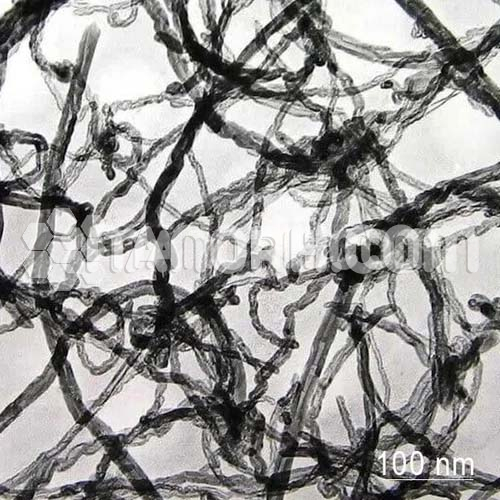
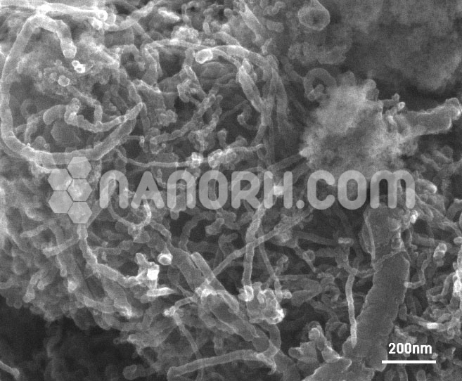
PVP Coated MWCNTs / Dry Solid Dispersible MWCNTs (>95%, OD: <7nm)
PVP Coated MWCNTs – Carbon nanotubes have incredible mechanical and electrical properties and are required to prompt numerous new materials and modern applications, yet to exploit their qualities they should be exceedingly and exclusively dispersed.
| PVP Coated MWCNTs / Dry Solid Dispersible MWCNTs | |
| Product No | NRE-36029 |
| CAS No. | NA |
| Purity | > 95 wt% |
| Average Diameter | <7 nm |
| Average Length | 10-30 um (TEM) |
| Special Surface Area(SSA) | > 500 m2/g (BET) |
| Tap Density | 0.27g/cm3 |
| True Density | 2.1 g/cm3 |
| Electric Conductivity | > 100 S/cm |
PVP Coated MWCNTs – Carbon nanotubes have incredible mechanical and electrical properties and are required to prompt numerous new materials and modern applications, yet to exploit their qualities they should be exceedingly and exclusively dispersed.
MWNTs are highly conductive when properly integrated into a composite structure. The outer wall alone is conducting, the inner walls are not significant to conductivity. MWNTs have a high aspect ratio with lengths typically more than 100 times the diameter, and much higher. Their performance and application are based not just on aspect ratio, but also on the degree of entanglement and the straightness of the tubes, which in turn is a function of both the degree and dimension of defects in the tubes.
MWNTs are suitable for various applications due to its high conductivity and high aspect ratio. The needed conductivity level can be achieved with much lesser loadings than for conventional solutions such as metal particulates or carbon black. Applications are electrostatic discharge protection in wafer processing fabrication, antistatic elastomeric and plastic components for automobile fuel line components, plastics rendered conductive to enable electrostatic spray painting of automobile body parts, RFI shielding materials, etc.
Multi-Walled Carbon Nanotubes (MWNTs, MWCNTs) Application
Potential applications of carbon nanotubes are: (1) additives in polymers; (2) catalysts; (3) electron field emitters for cathode ray lighting elements; (4) flat panel display; (5) gas-discharge tubes in telecom networks; (6) electromagnetic-wave absorption and shielding; (7) energy conversion; (8) lithium-battery anodes; (9) hydrogen storage; (10) nanotube composites (by filling or coating); (11) nanoprobes for STM, AFM, and EFM tips; (12) nanolithography; (13) nanoelectrodes; (14) drug delivery; (15) sensors; (16) reinforcements in composites; (17) supercapacitor.