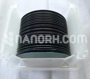
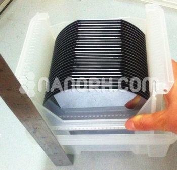
Silicon Carbide Wafer N Types
| Silicon Carbide Wafer N Types | |
| Product No | NRE-44024 |
| CAS | 409-21-2 |
| Type | N-Type |
| Doping | Phosphorous |
| Crystal method | CZ |
| Surface | Single Side Polished |
| Diameter (mm) | 2” (50.8mm) |
| Thickness | 275 μm |
| Resistivity | 1-10ohm-cm |
| Oxygen Contents | 12.5-16.5 ppma |
Silicon Carbide Wafer N Types
Introduction:
Silicon carbide wafer n types are semiconductor materials that have been doped with elements, such as phosphorus, that provide additional free electrons. This doping process creates an abundance of negatively charged carriers, enhancing the electrical conductivity of the silicon.
Applications
Integrated Circuits (ICs):
silicon n-type wafers are widely used in the production of integrated circuits, forming key components like transistors, diodes, and resistors that are crucial for various electronic functions.
Transistors:
They are particularly important in fabricating N-channel MOSFETs (Metal-Oxide-Semiconductor Field-Effect Transistors), which are integral to digital circuits for switching and amplification.
Photovoltaic Cells:
silicon n-type wafers are used in solar cell production, where they form junctions with p-type silicon to enhance the efficiency of light absorption and charge carrier collection.
Microelectromechanical Systems (MEMS):
These wafers are utilized in MEMS devices, such as accelerometers and pressure sensors, providing the necessary electrical properties for precise measurement and control.
Optoelectronic Devices:
Silicon N-type is employed in the fabrication of light-emitting diodes (LEDs) and laser diodes, enabling efficient electron-hole recombination for light emission.