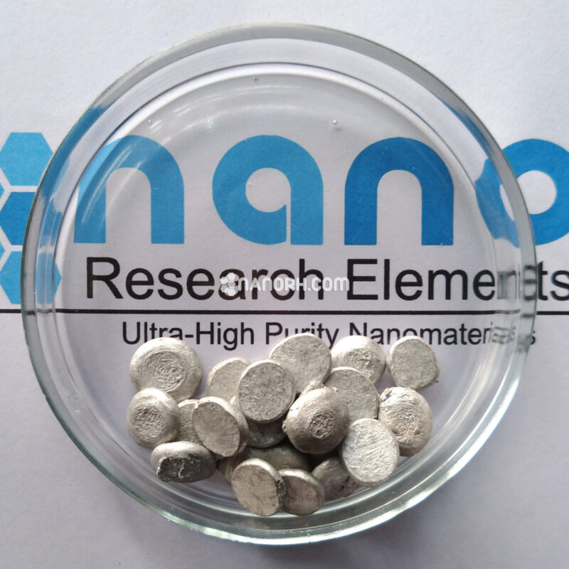
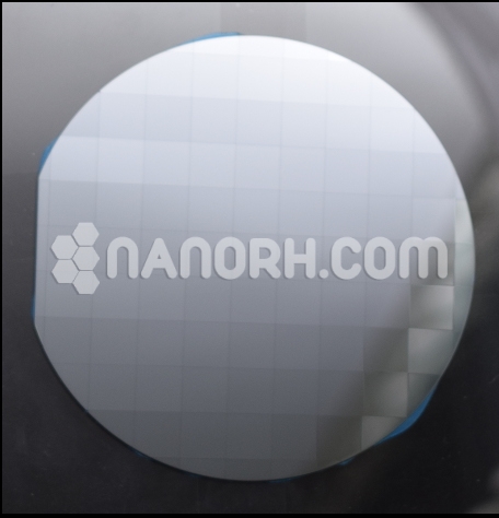
Silicon Wafer 6 inch
| Silicon Wafer 6 inch | |
| Product No | NRE-44029 |
| CAS | 7440-21-3 |
| Type | P-Type |
| Crystal method | CZ |
| Doping | Boron |
| Diameter (mm) | 6” (152.4mm) |
| Thickness | 250-500μm |
| Resistivity | 1-10ohm-cm |
| RRG (%) | ≤12 |
| Oxygen Contents (ppma) | 12.5-16.5 |
Silicon Wafer 6 inch
Introduction:
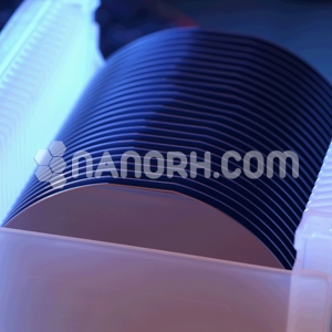
Silicon wafer 6 inch are thin, flat discs made of silicon crystals, commonly used as substrates in semiconductor manufacturing and various electronic applications. The 6-inch (150 mm) silicon wafer is a standard size in the semiconductor industry, playing a crucial role in the fabrication of integrated circuits (ICs), microelectromechanical systems (MEMS), and various optoelectronic devices.
Applications:
Integrated Circuits (ICs):
The 6-inch wafer can accommodate multiple dies, maximizing manufacturing efficiency.
Microelectromechanical Systems (MEMS):
Employed in devices that combine mechanical and electrical components at a microscale. Applications include accelerometers, gyroscopes, and sensors in automotive, consumer electronics, and medical devices.
Photovoltaics:
Utilized in solar cell manufacturing. Silicon wafers are essential for converting sunlight into electricity, making them vital for renewable energy solutions.
LED Technology:
Used as substrates for the production of light-emitting diodes (LEDs) and other optoelectronic components, supporting advancements in lighting and display technologies.
RF and Microwave Devices:
Integral in the fabrication of radio frequency (RF) and microwave components, which are crucial for communication technologies, including mobile phones and satellite systems.
Power Electronics:
Utilized in devices that manage and convert electrical power, playing a significant role in applications ranging from consumer electronics to electric vehicles.