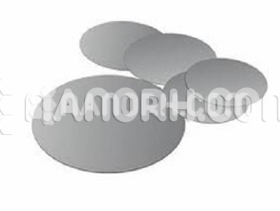
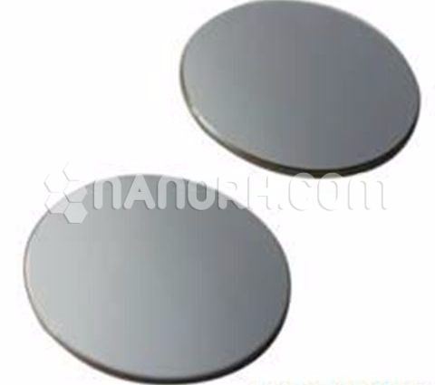
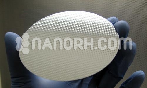
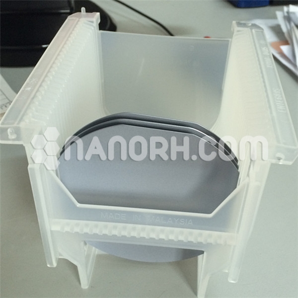
| Silicon Wafer N-Type | |
| Product No | NRE-44031 |
| CAS | 7440-21-3 |
| Type | N Type |
| Crystal method | NA |
| Doping | Phosphorous |
| Diameter (mm) | 4” (100mm) |
| Thickness | 525 ± 25 µm |
| RRG (%) | NA |
| Crystal Orientation | <100> |
| Oxygen Contents | NA |
| Carbon Contents | NA |
Silicon Wafer N Type
Introduction: Silicon wafer N-Type are a type of semiconductor wafer that is doped with elements that have more valence electrons than silicon, typically phosphorus, arsenic, or antimony. This doping process introduces extra electrons, resulting in an abundance of negatively charged carriers (electrons) in the material. Is crucial in the fabrication of various electronic devices due to its enhanced conductivity and specific electrical properties.
Applications:
Integrated Circuits (ICs):
Silicon wafer N-Type are widely used in the production of integrated circuits, forming essential components such as transistors, diodes, and other logic devices. They enable efficient electronic switching and signal processing.
Photovoltaic Cells:
Silicon wafer N-Type are used to create junctions with p-type materials, enhancing the efficiency of light absorption and electron flow, which improves overall solar cell performance.
Microelectromechanical Systems (MEMS):
Silicon wafer N type are employed in MEMS devices, including sensors and actuators, where precise control of electronic properties is required for effective operation.
LEDs and Laser Diodes:
Silicon wafer N type is used in the fabrication of light-emitting diodes (LEDs) and laser diodes, particularly in creating the necessary junctions for efficient light emission.
Power Electronics:
These wafers are essential in power electronic devices, such as MOSFETs (Metal-Oxide-Semiconductor Field-Effect Transistors), which are critical for managing and converting electrical power in various applications.


