| AgInS2 Sputtering Targets | |
| Product No | NRE-43300 |
| CAS No. | NA |
| Formula | AgInS2 |
| Molecular Weight | NA |
| Purity | >99.9% |
| Density | NA |
| Thickness | 3 mm ± 0.5mm (can be customized) |
| Diameter | 50 mm ± 1mm (can be customized) |
| Shape | Round |
| Resistivity | NA |
| Thermal Conductivity | NA |
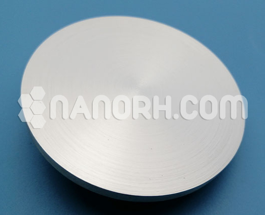
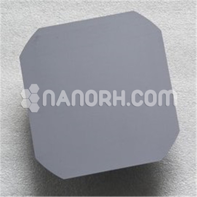
AgInS2 Sputtering Targets
Silver Indium Sulfide (AgInS₂) sputtering targets are used in various advanced technological applications due to their unique optical, electrical, and material properties.
Thin-Film Solar Cells:
Photovoltaic Devices: AgInS₂ Sputtering Targets is used in thin-film solar cells as an absorber layer material. It is a chalcopyrite semiconductor with a direct bandgap, making it suitable for converting sunlight into electricity. The material’s ability to absorb a broad spectrum of sunlight makes it an attractive option for increasing the efficiency of photovoltaic devices.
Optoelectronic Devices:
Photodetectors: AgInS₂ Sputtering Target is used in the fabrication of photodetectors, which are devices that convert light into an electrical signal. Its semiconducting properties make it ideal for detecting light in various wavelengths, including visible and near-infrared regions.
Light-Emitting Diodes (LEDs): The material is also used in some LED technologies, where it helps to produce light with specific wavelengths due to its tunable bandgap properties.
Semiconductor Research:
Material Development: AgInS₂ Sputering Targets sputtering targets are used in research and development of new semiconductor materials. Researchers explore its potential in creating novel electronic and optoelectronic devices due to its unique electrical and optical characteristics.
Heterojunction Devices: AgInS₂ is used in the development of heterojunction devices, where it forms a junction with other semiconductor materials to create devices with improved performance characteristics, such as better charge carrier separation and increased efficiency.
Photocatalysis:
Environmental Applications: AgInS₂ is employed in photocatalytic applications, such as water splitting and pollution degradation, where it acts as a catalyst under light irradiation. Its ability to absorb visible light and generate electron-hole pairs makes it effective for environmental cleanup processes.
Transparent Conductive Films:
Display Technology: AgInS₂ can be used to create transparent conductive films, which are essential in the manufacturing of display technologies such as touchscreens, LCDs, and OLEDs. These films conduct electricity while allowing light to pass through, enabling the operation of displays.


