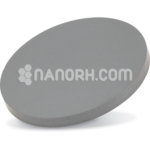
| Cadmium Arsenide Sputtering Targets | |
| Product No | NRE-43344 |
| CAS No. | 12006-15-4 |
| Formula | Cd3As2 |
| Molecular Weight | 487.08 |
| Purity | >99.9% |
| Density | 3.03 |
| Thickness | 3 mm ± 0.5mm (can be customized) |
| Diameter | 50 mm ± 1mm (can be customized) |
| Shape | Round |
| Resistivity | NA |
| Thermal Conductivity | NA |
Cadmium Arsenide Sputtering Targets
Cadmium arsenide (Cd₃As₂) sputtering targets are used for depositing thin films of cadmium arsenide, a compound semiconductor with notable electronic and optical properties.
Semiconductor Devices
High-Mobility Transistors: Cadmium arsenide is used in high-mobility transistor devices due to its high electron mobility. Sputtered Cd₃As₂ films can be used to fabricate these transistors, which are critical for high-speed electronic applications.
Photodetectors: Cd₃As₂ can be used in photodetectors for infrared and visible light. Sputtered films are used in devices that require high sensitivity to light, such as optical sensors and imaging systems.
Optoelectronic Devices
Infrared Detectors: Due to its optical properties, cadmium arsenide is suitable for infrared detection. Sputtered Cd₃As₂ films are used in infrared detectors and thermal imaging systems.
Light Emitting Devices: Cadmium arsenide can be used in light-emitting devices, including LEDs, particularly for specific wavelengths within the infrared spectrum.
Solar Cells
Thin-Film Photovoltaics: Cadmium arsenide films can be used in thin-film solar cells. The material’s electronic properties make it a good candidate for photovoltaic applications, where sputtered Cd₃As₂ layers can be used to create efficient solar cell components.
Semiconductor Thin-Film Transistors (TFTs)
Display Technology: Cadmium arsenide sputtered films can be used in thin-film transistors for displays, such as LCDs and OLEDs. The high mobility of Cd₃As₂ improves the performance and response time of the displays.
High-Speed Electronics
RF and Microwave Devices: Due to its high electron mobility, cadmium arsenide is used in radio-frequency (RF) and microwave devices. Sputtered Cd₃As₂ layers can be used to fabricate components that operate at high frequencies.
Research and Development
Material Science Research: Cd₃As₂ sputtering targets are used in research and development to explore new applications and understand the fundamental properties of cadmium arsenide. Researchers use these targets to investigate the material’s behavior in different devices and conditions.
Specialty Sensors
Gas Sensors: Cd₃As₂ films can be used in specialty sensors for detecting specific gases, due to the material’s unique electronic properties. Sputtering allows precise deposition of the film for optimal sensor performance.


