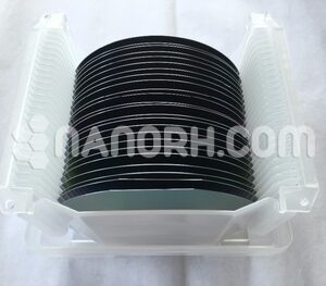
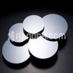
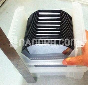
Cadmium Zinc Telluride Sputtering Targets
Cadmium Zinc Telluride Sputtering Targets
| Cadmium Zinc Telluride Sputtering Targets | |
| Product No | NRE-43349 |
| CAS No. | NA |
| Formula | CZT |
| Molecular Weight | NA |
| Purity | >99.9% |
| Density | NA |
| Thickness | 3 mm ± 0.5mm (can be customized) |
| Diameter | 50 mm ± 1mm (can be customized) |
| Shape | Round |
| Resistivity | NA |
| Thermal Conductivity | NA |
Cadmium Zinc Telluride Sputtering Targets
Copper zinc telluride sulfide (Cu₂ZnSnS₄ or CZTS) sputtering targets are used in several advanced applications due to the unique properties of this material. CZTS is a promising semiconductor material with favorable characteristics for various technological uses.
Thin-Film Solar Cells
Application: CZTS is used as an absorber layer in thin-film solar cells. It is a key material in photovoltaic technology, often combined with other layers to form efficient solar panels.
Benefit: Provides a direct bandgap and high absorption coefficient, leading to efficient light absorption and conversion into electrical energy. It’s also known for being environmentally friendly and cost-effective compared to other materials like cadmium telluride.
Photodetectors
Application: CZTS thin films are used in photodetectors for detecting light in various wavelength ranges.
Benefit: Offers good photoresponse characteristics, making it suitable for imaging systems and optical communication.
Semiconductors for Electronic Devices
Application: CZTS can be used as a semiconductor material in electronic devices, including thin-film transistors and other semiconductor components.
Benefit: Provides good electronic properties, such as high mobility and stability, which are crucial for reliable electronic performance.
Thermoelectric Materials
Application: CZTS thin films are explored for use in thermoelectric materials, which convert heat directly into electrical energy or are used for cooling applications.
Benefit: Offers suitable thermoelectric properties, including good electrical conductivity and low thermal conductivity, for efficient energy conversion.
Optoelectronic Devices
Application: CZTS is utilized in various optoelectronic devices, such as light-emitting diodes (LEDs) and photodetectors.
Benefit: Enhances device performance due to its advantageous optical and electrical properties, improving efficiency and functionality.
Catalysts
Application: CZTS thin films are studied for use as catalysts in various chemical reactions, including those for environmental remediation and synthetic chemistry.
Benefit: Provides catalytic activity that can improve reaction efficiency and selectivity.
Environmental Sensors
Application: CZTS is used in the fabrication of environmental sensors for detecting gases or other environmental parameters.
Benefit: Offers high sensitivity and accuracy in detecting specific environmental changes.