Copper Indium Selenide Sputtering Targets
Copper Indium Selenide Sputtering Targets
| Copper Indium Selenide Sputtering Targets | |
| Product No | NRE-43395 |
| CAS No. | 12018-95-0 |
| Formula | CuInSe2 |
| Molecular Weight | 336.28 |
| Purity | >99.9% |
| Density | NA |
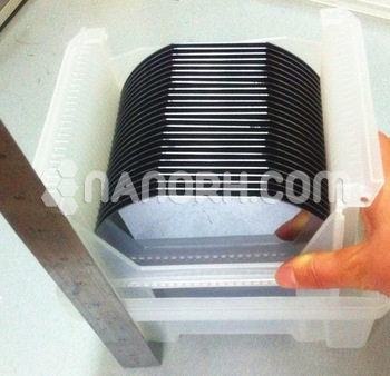
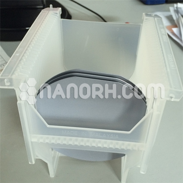
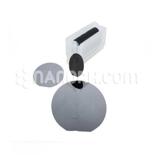
| Thickness | 3 mm ± 0.5mm (can be customized) |
| Diameter | 50 mm ± 1mm (can be customized) |
| Shape | Round |
| Resistivity | NA |
| Thermal Conductivity | NA |
Copper Indium Selenide Sputtering Targets
Copper indium selenide (CuInSe₂) sputtering targets are used in several advanced technological applications, primarily due to their excellent semiconductor and photovoltaic properties. Here’s an overview of their main applications..
Photovoltaic Solar Cells
Thin-Film Solar Panels: CuInSe₂ is a key material in the production of high-efficiency thin-film solar cells. These cells are known for their excellent light absorption properties and high power conversion efficiency. CuInSe₂ serves as the absorber layer in these cells, converting sunlight into electricity effectively.
High-Efficiency Devices: CuInSe₂-based solar cells can achieve high efficiencies, making them competitive with other thin-film technologies and even silicon-based solar panels.
Optoelectronic Devices
Light Sensors and Detectors: CuInSe₂ can be used in optoelectronic devices such as photodetectors and light sensors. Its ability to absorb and convert light into electrical signals makes it suitable for these applications.
Light Emitting Devices: The material’s properties can also be utilized in light-emitting devices, including LEDs and laser diodes, where specific optical characteristics are required.
Thin-Film Transistors (TFTs)
Display Technology: CuInSe₂ is sometimes used in the fabrication of thin-film transistors, which are critical components in liquid crystal displays (LCDs) and organic light-emitting diodes (OLEDs). The material’s semiconductor properties contribute to the performance of these displays.
Research and Development
Material Science: CuInSe₂ sputtering targets are employed in research to explore new materials and improve existing technologies. This includes studying the effects of different compositions and deposition techniques on film quality and device performance.
Energy-Efficient Coatings
Specialized Coatings: CuInSe₂ can be used to produce coatings with specific electronic or optical properties. These coatings can be applied in various applications, including energy-efficient windows and other advanced optical devices.
Advantages of CuInSe₂:
High Absorption Efficiency: CuInSe₂ has a high absorption coefficient, which allows it to absorb a large amount of sunlight with a relatively thin layer. This is advantageous for creating efficient thin-film solar cells.
Stable Performance: CuInSe₂ solar cells have good stability and performance over time, making them suitable for long-term applications in various environments.
Flexibility: Thin films made from CuInSe₂ can be deposited on flexible substrates, expanding their potential applications beyond rigid panels.
In summary, CuInSe₂ sputtering targets are primarily used in the production of high-efficiency thin-film solar cells and various optoelectronic devices.