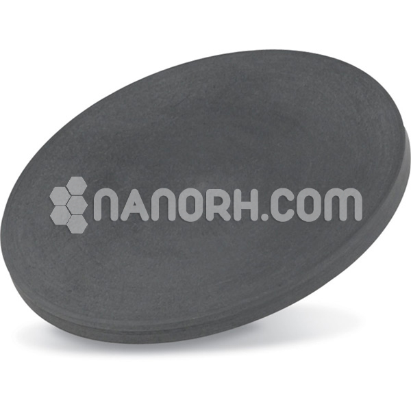
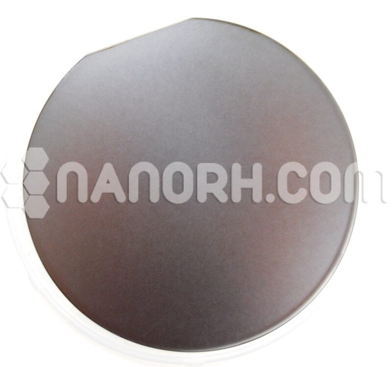
| GaAsSe Sputtering Targets | |
| Product No | NRE-43415 |
| CAS No. | NA |
| Formula | GaAsSe |
| Molecular Weight | NA |
| Purity | >99.9% |
| Density | NA |
| Thickness | 3 mm ± 0.5mm (can be customized) |
| Diameter | 50 mm ± 1mm (can be customized) |
| Shape | Round |
| Resistivity | NA |
| Thermal Conductivity | NA |
GaAsSe Sputtering Targets
GaAsSe (Gallium Arsenide Selenide) sputtering targets are used in thin film deposition processes and have specific applications due to their unique properties. Here’s an overview of their applications and considerations.
Applications
Optoelectronics:
Photodetectors: GaAsSe can be used in the production of photodetectors that operate in the infrared spectrum.
Light-Emitting Diodes (LEDs): Thin films of GaAsSe may be used in the fabrication of LEDs with specific wavelengths.
Solar Cells:
Photovoltaics: GaAsSe can be used in the development of thin-film solar cells, especially those designed for high-efficiency applications or specialized spectral absorption.
Semiconductors:
Semiconductor Devices: Used in the production of various semiconductor devices, including high-speed electronic components and integrated circuits.
Nonlinear Optical Devices:
Optical Nonlinearities: GaAsSe materials can exhibit nonlinear optical properties, making them useful in devices that require frequency doubling or other nonlinear optical effects.
Laser Materials:
Laser Thin Films: GaAsSe can be used as a component in laser materials, particularly in the context of solid-state lasers with specific wavelength requirements.
Sputtering Process
Sputtering Technique: In the sputtering process, ions from a plasma are directed at the GaAsSe target, causing atoms to be ejected and then deposited onto a substrate to form a thin film.
Target Composition: The GaAsSe target must be carefully prepared to ensure the correct stoichiometric ratio of gallium (Ga), arsenic (As), and selenium (Se) to achieve the desired film properties.


