Our Products

Gallium Antimonide Sputtering Targets
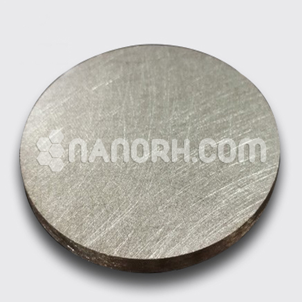
Gallium Antimonide Sputtering Targets
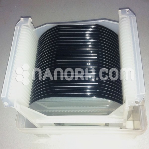
Gallium Antimonide Sputtering Targets
Product No NRE-43419
CAS No. 12064-03-8
Formula GaSb
Molecular Weight 191.48
Purity >99.9%
Density 5.614 g/cm3
Thickness 3 mm ± 0.5mm (can be customized)
Diameter 50 mm ± 1mm (can be customized)
Shape Round
Resistivity NA
Thermal Conductivity NA

Gallium Antimonide Sputtering Targets
Gallium antimonide (GaSb) sputtering targets are used in various advanced applications due to their unique electronic and optical properties. Here’s an overview of their applications and considerations.

Applications

Semiconductors:

Infrared Detectors: GaSb is widely used in the production of infrared (IR) detectors and photodetectors. Its ability to detect IR radiation makes it suitable for applications in thermal imaging and night vision.

Semiconductor Devices: GaSb is used in various semiconductor devices, including high-speed and high-frequency electronics. It can be used in the fabrication of transistors and other electronic components.

Example: IR detectors in military and surveillance systems, high-frequency transistors in communication devices.

Optoelectronics:

Light Emitting Diodes (LEDs): GaSb is used in the production of LEDs that emit in the infrared spectrum. This is valuable for communication systems and other optoelectronic applications.

Laser Diodes: GaSb can be used in the production of laser diodes, particularly those operating in the infrared region.

Example: LEDs and laser diodes used in fiber-optic communication systems and other IR applications.

Thermoelectric Devices:

Thermoelectric Materials: GaSb is used in thermoelectric devices where it can convert heat into electrical energy or vice versa. Its properties can be tailored for specific temperature ranges and performance requirements.

Example: Thermoelectric generators or coolers used in power generation or temperature control applications.

Alloy Systems:

Gallium Antimonide Alloys: GaSb is often used in alloy systems with other materials, such as indium antimonide (InSb), to create materials with tailored electronic properties for specialized applications.

Example: Materials used in high-performance electronics or optoelectronics where precise control of electronic band structure is required.

High-Speed Electronics:

High Electron Mobility Transistors (HEMTs): GaSb-based materials are used in high-speed and high-frequency transistors due to their high electron mobility.

Example: Transistors used in radio frequency (RF) and microwave applications.

Sputtering Process

Sputtering Technique: In the sputtering process, ions are directed at the GaSb target in a vacuum chamber, causing atoms to be ejected from the target and deposit onto a substrate to form a thin film.

Target Composition: The target material must be of high purity to ensure uniform deposition and high-quality film properties. Any impurities can affect the performance and characteristics of the deposited films.


error: