Germanium Sputtering Target (Ge, Purity: 99.99%)
Germanium Sputtering Target
| Germanium Sputtering Target | |
| Product No | NRE-43057 |
| CAS No. | 7440-56-4 |
| Formula | Ge |
| Molecular Weight | 72.61 g/mol |
| Purity | 99.99% |
| Density | 5.323 g/cm³ |
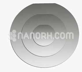
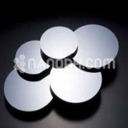
| Thickness | 3 mm ± 0.5mm (can be customized) |
| Diameter | 50 mm ± 1mm (can be customized) |
| Shape | Round |
| Resistivity | NA |
| Thermal Expansion | NA |
Germanium Sputtering Target
Germanium sputtering targets are specialized materials used to create thin films of germanium through the sputtering process, a physical vapor deposition (PVD) technique. These targets are typically made from high-purity germanium and are crucial for producing films with specific electrical, optical, and mechanical properties.
Germanium sputtering target a semiconductor with a bandgap of approximately 0.66 eV, has unique characteristics that make it highly desirable for a variety of applications in modern technology. Its compatibility with silicon and excellent charge carrier mobility are particularly noteworthy, enabling the development of high-performance electronic devices.
Applications
Semiconductor Devices: Ge is used in high-speed transistors and diodes, playing a vital role in enhancing the performance of electronic circuits.
Thin-Film Transistors (TFTs): In displays and flexible electronics, germanium films improve charge carrier mobility, resulting in better performance and efficiency.
Photovoltaics: Ge is essential in multi-junction solar cells, where it serves as a bottom cell layer, enhancing overall solar energy conversion efficiency.
Optoelectronics: Germanium films are utilized in photodetectors and infrared sensors, benefiting from their sensitivity in the infrared spectrum.
Microelectromechanical Systems (MEMS): Germanium is incorporated in MEMS devices for its mechanical properties and compatibility with silicon technology.
Thermoelectric Applications: Ge can be used in thermoelectric devices to convert temperature differences into electrical energy, making it useful for energy harvesting.