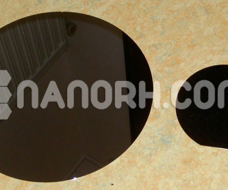
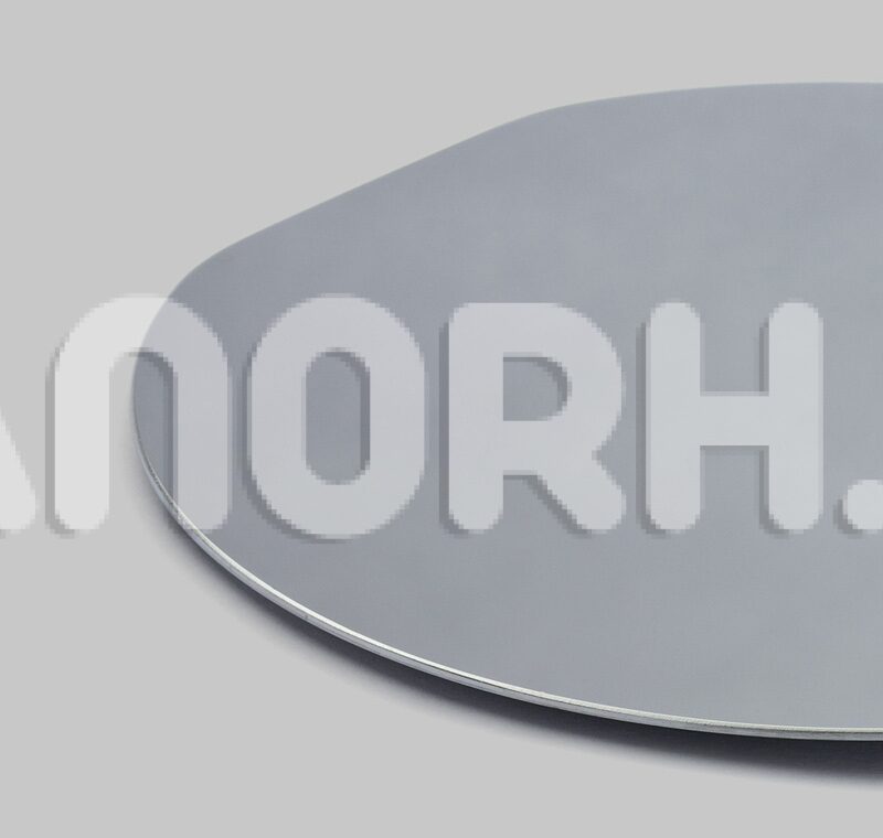
Silicon Wafer 4 inch P Type (Platinum/Tantalum/Silicon)
| Silicon Wafer 4 inch P Type | |
| Product No | NRE-44028 |
| CAS | 7440-21-3 |
| Type | P-Type |
| Crystal Orientation | <100> |
| Carbon Contents (ppma) | ≤1 |
| Doping | (Pt/Ta/Si) |
| Diameter (mm) | 4” (101.6mm) |
| Thickness | 275 μm |
| Resistivity | 1-10ohm-cm |
| Surface | Single Side Polished |
Silicon Wafer 4 inch P Type
Introduction
Silicon wafer 4 inch p type that are doped with elements such as boron and feature platinum and tantalum coatings represent advanced semiconductor materials used in a variety of high-performance applications. The p-type doping introduces “holes” (positive charge carriers) into the silicon lattice, enhancing its electrical properties. The addition of platinum and tantalum as coatings or layers contributes to improved functionality, such as enhanced conductivity and stability.
Properties
Electrical Conductivity: P-type doping with boron increases the hole concentration, making the silicon wafer suitable for various electronic applications.
Surface Coating Benefits: The platinum and tantalum coatings provide excellent thermal and chemical stability, enhancing the wafer’s durability and performance in demanding environments.
High Thermal Conductivity: Both platinum and tantalum have high thermal conductivity, which aids in efficient heat dissipation during device operation.
Compatibility: The wafers can be easily integrated into existing semiconductor fabrication processes.
Applications
Integrated Circuits (ICs):
Used in the manufacturing of various ICs, including analog and mixed-signal devices, where p-type silicon is crucial for forming p-n junctions.
Power Electronics:
Employed in power devices such as bipolar junction transistors (BJTs) and thyristors, which require efficient charge transport and thermal management.
MEMS Devices:
Suitable for microelectromechanical systems (MEMS) applications, where the mechanical and electrical properties of the wafers are exploited for sensors and actuators.
Solar Cells:
Used as substrates in photovoltaic cells, contributing to the formation of effective p-n junctions for light absorption and energy conversion.
Sensors:
Employed in various sensor technologies, including temperature and pressure sensors, benefiting from the wafers’ sensitivity and response characteristics.
Optoelectronic Devices:
Utilized in the production of light-emitting diodes (LEDs) and laser diodes, where p-type silicon is essential for device functionality.
Thin-Film Technologies:
Suitable for applications in thin-film transistors and other devices that require high-quality substrates.