InSbTe Sputtering Targets
InSbTe Sputtering Targets
| InSbTe Sputtering Targets | |
| Product No | NRE-43452 |
| CAS No. | NA |
| Formula | InSbTe |
| Molecular Weight | NA |
| Purity | >99.9% |
| Density | NA |
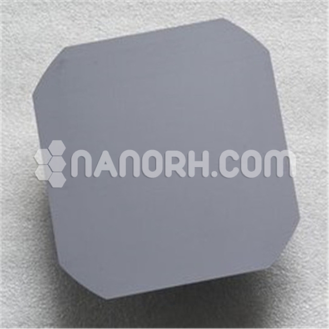
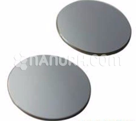
| Thickness | 3 mm ± 0.5mm (can be customized) |
| Diameter | 50 mm ± 1mm (can be customized) |
| Shape | Round |
| Resistivity | NA |
| Thermal Conductivity | NA |
InSbTe Sputtering Targets
InSbTe sputtering targets are used in various applications primarily in thin film deposition processes, particularly in the semiconductor, optics, and solar cell industries. Here are some key applications.
Semiconductors: In semiconductor fabrication, sputtering is employed to deposit metal films, insulating layers, and dielectric materials on wafers. In-situ targets can enhance film quality and uniformity.
Optical Coatings: Sputtering is used to create thin films for anti-reflective coatings, mirrors, and other optical components. In-situ targets help achieve precise control over film properties.
Solar Cells: In the production of photovoltaic cells, sputtering targets are used to deposit conductive and absorptive layers, contributing to improved efficiency and performance.
Magnetic Storage Media: Sputtering is utilized to create magnetic layers in hard drives and other storage devices, where in-situ targets improve magnetic properties and thickness uniformity.
Decorative Coatings: In industries like automotive and fashion, sputtering provides aesthetic coatings that are durable and have specific colors or finishes.
MEMS Devices: Micro-electromechanical systems (MEMS) rely on sputtered materials for components such as sensors and actuators.
.