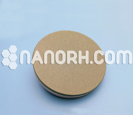
| IZO Sputtering Target | |
| Product No | NRE-43078 |
| CAS No. | 117944-65-7 |
| Formula | In2O3 / ZnO |
| Molecular Weight | NA |
| Purity | 99.9% |
| Density | NA |
| Thickness | 3 mm ± 0.5mm (can be customized) |
| Diameter | 50 mm ± 1mm (can be customized) |
| Shape | Round |
| Electrical Resistivity | NA |
| Electronegativity | NA |
IZO Sputtering Target
Introduction
Indium zinc oxide (IZO) is a semiconductor material composed of indium oxide (In₂O₃) and zinc oxide (ZnO). IZO sputtering targets are utilized in the sputtering deposition process to create thin films of indium zinc oxide on various substrates. This material combines the properties of both indium and zinc oxides, resulting in excellent electrical conductivity, optical transparency, and good thermal stability. IZO is particularly valued in applications that require transparent conducting oxides (TCOs).
Applications
Transparent Conductive Films:
IZO is widely used in the production of transparent conductive films for display technologies, such as liquid crystal displays (LCDs) and organic light-emitting diodes (OLEDs). Its high optical transparency and electrical conductivity make it ideal for these applications.
Solar Cells:
IZO is utilized in thin-film solar cells, where it serves as a transparent front contact layer, helping to improve the efficiency of light absorption and electrical conduction.
Touchscreen Technologies:
IZO thin films are employed in touch-sensitive devices due to their conductivity and transparency, facilitating the functionality of touchscreens in smartphones, tablets, and other devices.
Electronics:
IZO is used in various electronic devices, including sensors and integrated circuits, where its conductive and semiconducting properties are beneficial.
Optical Coatings:
The optical properties of IZO make it suitable for various optical coatings, including anti-reflective layers and mirrors in optical devices.
Research and Development:
IZO films are frequently used in research settings to study their unique properties and to develop new materials and devices, particularly in the fields of nanotechnology and optoelectronics.


