Niobium Arsenide Sputtering Targets
Niobium Arsenide Sputtering Targets
| Niobium Arsenide Sputtering Targets | |
| Product No | NRE-43524 |
| CAS No. | 12255-08-2 |
| Formula | NbAs |
| Molecular Weight | 167.82 |
| Purity | >99.9% |
| Density | NA |
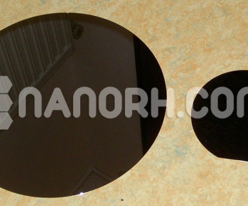
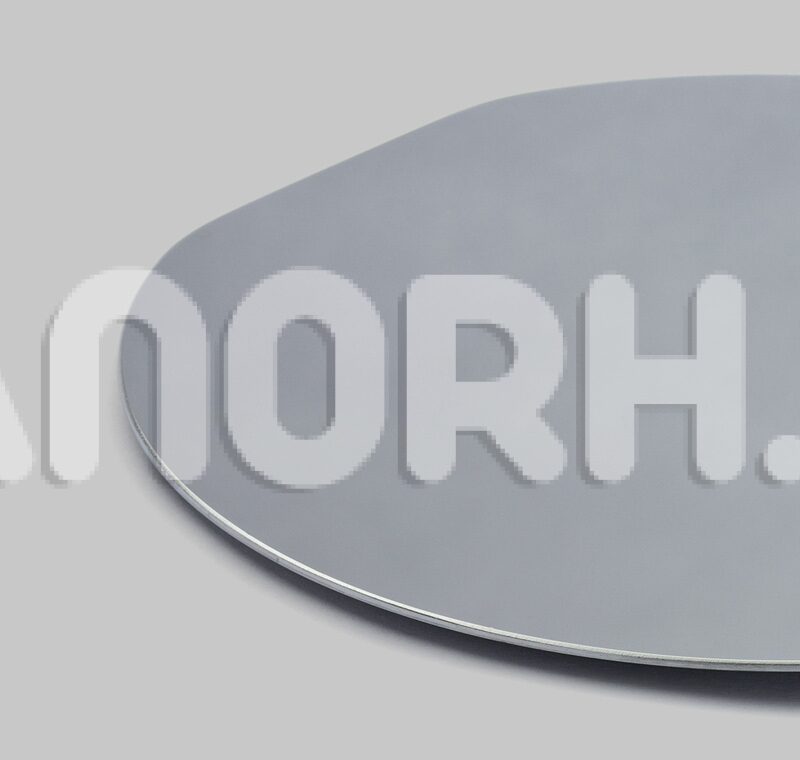
| Thickness | 3 mm ± 0.5mm (can be customized) |
| Diameter | 50 mm ± 1mm (can be customized) |
| Shape | Round |
| Resistivity | NA |
| Thermal Conductivity | NA |
Niobium Arsenide Sputtering Targets
Introduction:
Niobium arsenide sputtering targets is a compound of niobium and arsenic, notable for its unique electrical and physical properties. It has gained interest in various technological applications, particularly in the field of thin-film deposition through sputtering. Sputtering is a physical vapor deposition (PVD) technique that involves ejection of material from a target onto a substrate, allowing for the formation of thin films with specific properties.
Applications:
Semiconductor Devices: NbAs is explored for use in semiconductor applications due to its semiconductor-like behavior. It can be used to fabricate thin films for transistors and other electronic components.
Superconductors: Niobium-based compounds are known for their superconducting properties. NbAs can be studied for potential use in superconducting thin films, which are critical in applications such as quantum computing and magnetic resonance imaging (MRI).
Optoelectronic Devices: The unique optical properties of NbAs make it suitable for use in optoelectronic devices, including photodetectors and light-emitting diodes (LEDs).
Hard Coatings: Niobium and its compounds can provide wear-resistant coatings for tools and machinery, enhancing durability and performance in harsh environments.
Thermal and Electrical Conductors: NbAs can be utilized in applications requiringhigh thermal and electrical conductivity, contributing to efficient heat dissipation in electronic devices.
Conclusion
Niobium arsenide sputtering targets represent an important material for advanced technological applications, particularly in electronics and materials science.