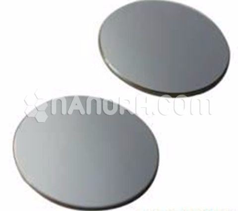
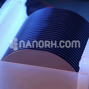
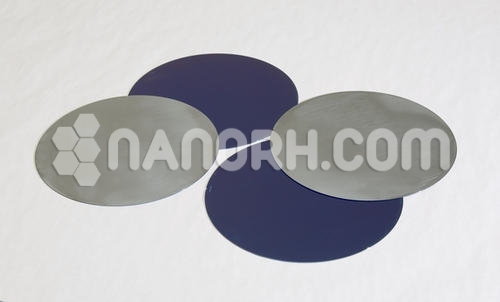
Silicon Wafer P Type (4 inch, Boron Doped)
| Silicon Wafer P Type | |
| Product No | NRE-44036 |
| CAS | 7440-21-3 |
| Type | P Type |
| Crystal method | NA |
| Doping | Boron |
| Diameter (mm) | 4” (100mm) |
| Thickness | 525 ± 25 µm |
| RRG (%) | NA |
| Crystal Orientation | <100> |
Silicon Wafer P Type (4 inch, Boron Doped)
Introduction
silicon wafer refers to a type of silicon (Si) wafer that has been doped with an element, typically boron (B), to create an excess of holes (positive charge carriers). In the context of semiconductors, a “hole” refers to the absence of an electron in the crystal lattice, effectively behaving as a positive charge.
Silicon Wafer: Silicon wafers are thin slices of silicon, typically ranging in size from a few inches to several inches in diameter, that serve as the substrate for fabricating integrated circuits (ICs) or other microelectronic devices. Silicon is the most widely used material for semiconductor devices due to its favorable electrical properties and abundant availability.
P-Type Doping: Doping refers to the intentional introduction of impurities into a semiconductor to change its electrical properties. In P-type doping, boron atoms (with fewer valence electrons than silicon) replace silicon atoms in the crystal lattice. This creates “holes” or vacancies in the lattice, which allow electrical current to flow as positive charge carriers.
4-inch Wafer: This refers to the diameter of the silicon wafer. A 4-inch wafer is a commonly used size for research, development, and small-volume production of semiconductor devices. Larger wafers (e.g., 6-inch, 8-inch, or more) are typically used in large-scale manufacturing.