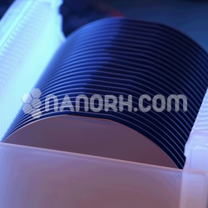
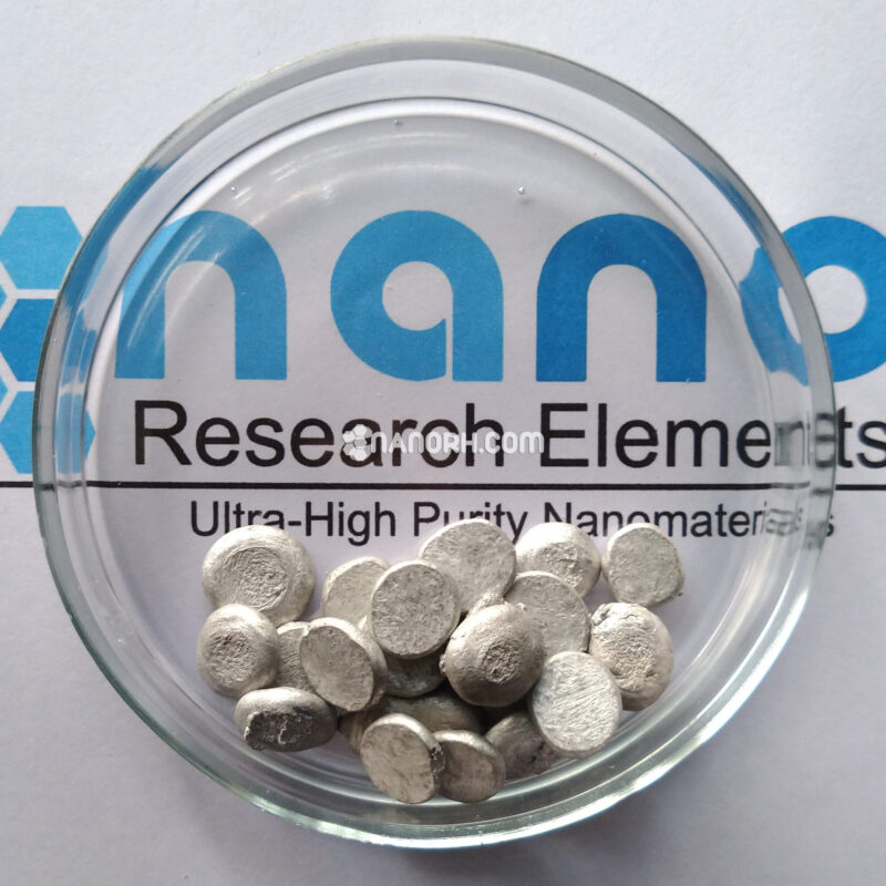
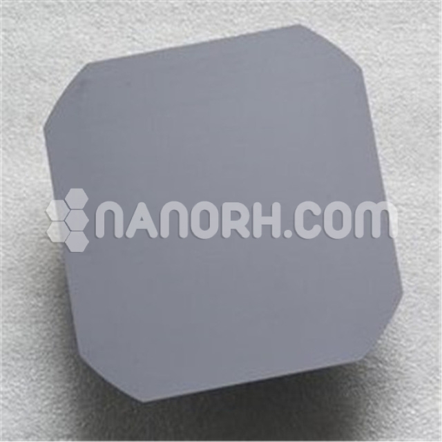
Tungsten Selenide Sputtering Targets
Tungsten Selenide Sputtering Targets
| Tungsten Selenide Sputtering Targets | |
| Product No | NRE-43593 |
| CAS No. | 12067-46-8 |
| Formula | WSe2 |
| Molecular Weight | 341.76 |
| Purity | >99.9% |
| Density | 9.32 g/cm3 |
| Thickness | 3 mm ± 0.5mm (can be customized) |
| Diameter | 50 mm ± 1mm (can be customized) |
| Shape | Round |
| Resistivity | NA |
| Thermal Conductivity | NA |
Tungsten Selenide Sputtering Targets
Introduction:
Tungsten selenide sputtering targets is a transition metal dichalcogenide known for its unique properties, including a layered structure, excellent electrical conductivity, and semiconductor characteristics. It has gained significant attention in recent years for its potential applications in electronics, optoelectronics, and materials science. Sputtering targets made from tungsten selenide are used in physical vapor deposition (PVD) processes to create high-quality thin films with tailored properties for various applications.
Applications
Electronics: WSe₂ is utilized in the fabrication of electronic devices, such as field-effect transistors (FETs), benefiting from its semiconducting properties and high mobility of charge carriers.
Optoelectronic Devices: Tungsten selenide is employed in photodetectors, light-emitting devices, and solar cells, where its optical properties contribute to improved efficiency and performance.
Flexible Electronics: Due to its layered structure, WSe₂ can be integrated into flexible electronic devices, paving the way for innovations in wearable technology and flexible displays.
Energy Storage: Tungsten selenide is explored for applications in batteries and supercapacitors, where its conductivity and surface properties enhance energy storage capabilities.
Catalysis: WSe₂ can serve as a catalyst or catalyst support in various chemical reactions, particularly in hydrogen evolution and other electrochemical processes.