| ZnAs2 Sputtering Targets | |
| Product No | NRE-43629 |
| CAS No. | NA |
| Formula | ZnAs2 |
| Molecular Weight | NA |
| Purity | >99.9% |
| Density | NA |
| Thickness | 3 mm ± 0.5mm (can be customized) |
| Diameter | 50 mm ± 1mm (can be customized) |
| Shape | Round |
| Resistivity | NA |
| Thermal Conductivity | NA |
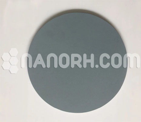
ZnAs2 Sputtering Targets
Introduction
ZnAs2 sputtering targets is a compound semiconductor that has garnered interest due to its unique electrical and optical properties. ZnAs₂ sputtering targets are used in physical vapor deposition (PVD) processes to create thin films of zinc arsenide on various substrates. These films are essential for various applications in electronics, optoelectronics, and photonics.
Applications
Semiconductor Devices: ZnAs₂ is used in the fabrication of semiconductor devices, such as diodes and transistors, benefiting from its direct bandgap properties.
Optoelectronic Devices: The compound is useful in optoelectronic applications, including light-emitting diodes (LEDs) and laser diodes, where efficient light emission and absorption are critical.
Solar Cells: ZnAs₂ can be used in thin-film solar cells, contributing to efficient light absorption and conversion, making it a candidate for renewable energy applications.
Infrared Detectors: Due to its semiconductor properties, ZnAs₂ is applicable in infrared detection technologies, enhancing the sensitivity and efficiency of detection systems.
Research and Development: ZnAs₂ films are also explored in academic and industrial research for novel applications in materials science and device engineering.
Sensors: ZnAs₂-based materials can be used in sensors for detecting gases or other environmental factors due to their semiconductor characteristics.


