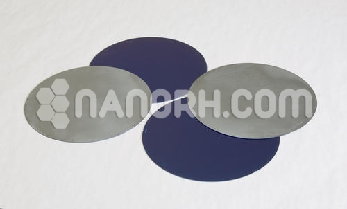
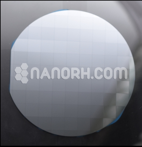
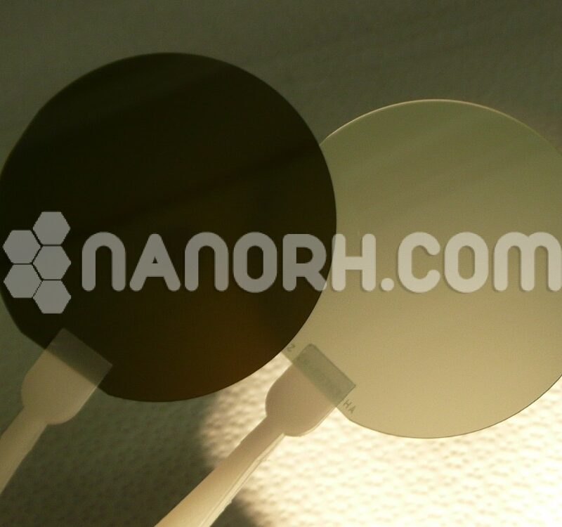
Ytterbium Sputtering Target
Ytterbium Sputtering Target
| Ytterbium Sputtering Target | |
| Product No | NRE-43176 |
| CAS No. | 7440-64-4 |
| Formula | Yb |
| Molecular Weight | 173.04 g/mol |
| Purity | 99.99% |
| Thickness | 3 mm ± 0.5mm (can be customized) |
| Diameter | 50 mm ± 1mm (can be customized) |
| Shape | Round |
Ytterbium Sputtering Target
Introduction:
Ytterbium sputtering target is a rare earth element known for its unique physical and chemical properties, including high thermal stability and good conductivity. As a sputtering target, pure ytterbium is used in thin film deposition processes, where it can be utilized to create high-quality films for various advanced applications. Ytterbium’s versatility makes it an important material in modern technology.
Applications:
Semiconductor Manufacturing:
Ytterbium is used in the fabrication of thin films for electronic devices, including transistors and diodes. Its unique electrical properties enhance device performance.
Optical Coatings:
Employed in the production of coatings for optical components such as lenses and mirrors, enhancing light transmission and reducing reflection.
Laser Technology:
Ytterbium is often used as a dopant in solid-state lasers, improving efficiency and output power. Thin films of ytterbium can be crucial in the development of high-performance laser systems.
Magnetic Materials:
Utilized in the production of magnetic films for data storage applications and spintronics, where the manipulation of electron spin is essential.
Thermal Barrier Coatings:
Ytterbium sputtering targets can be used to produce thermal barrier coatings that improve the performance of components in high-temperature environments, such as turbine blades in aerospace applications.
Biomedical Applications:
Involved in the development of biocompatible coatings for medical devices, improving compatibility and performance in biomedical applications.