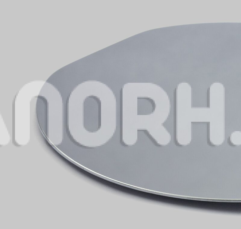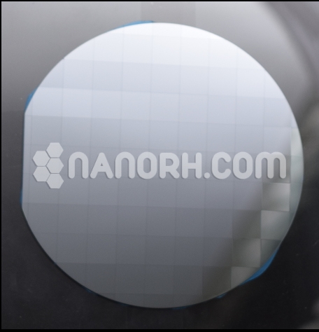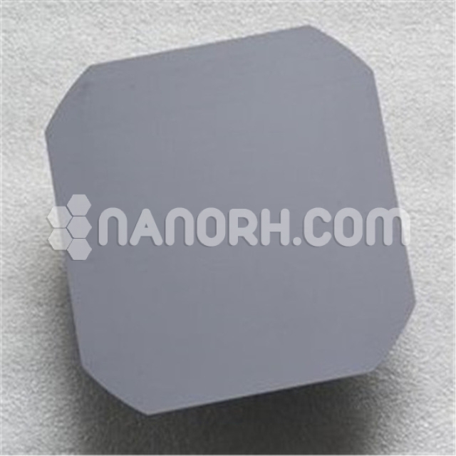
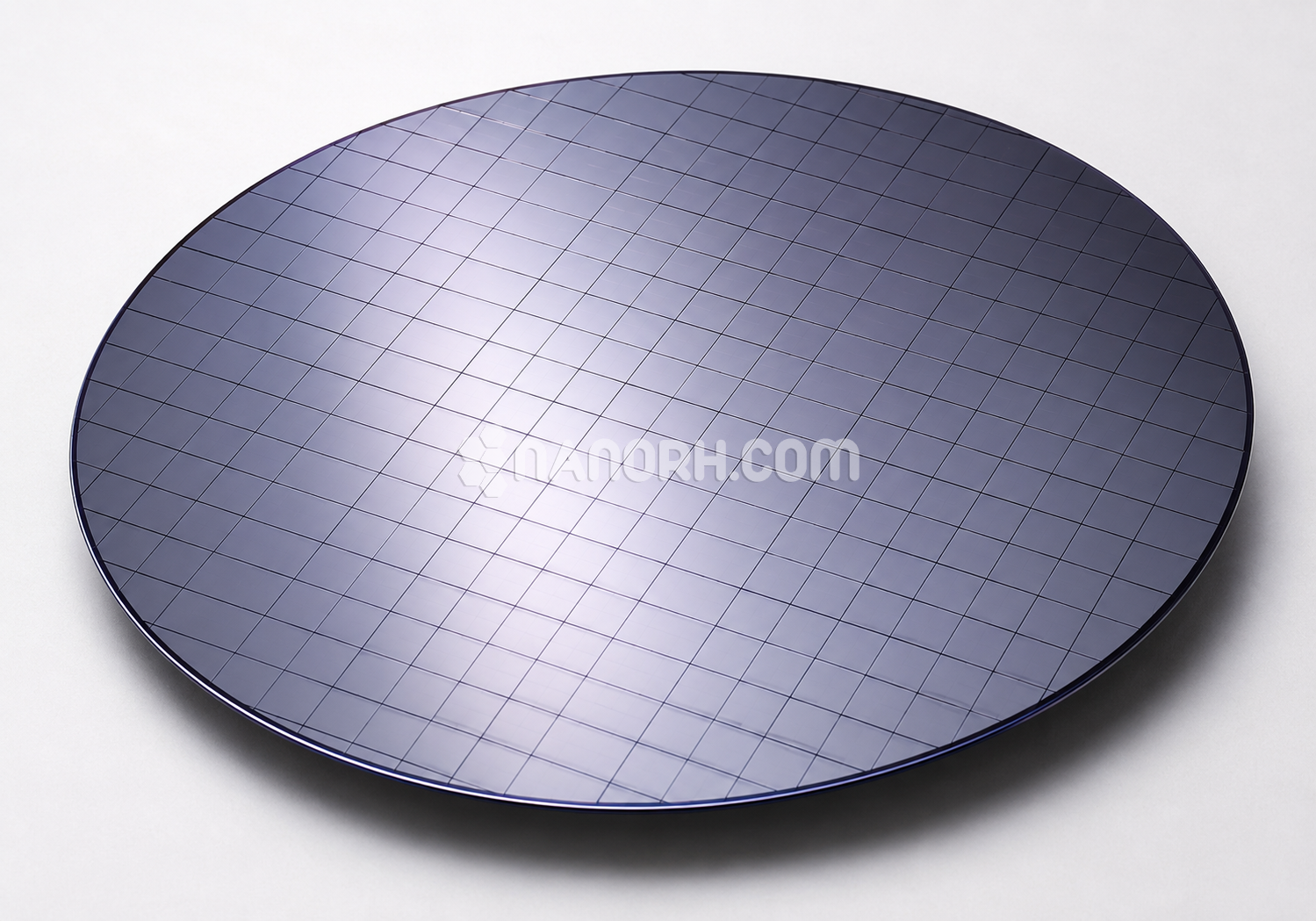
Monocrystalline Silicon Wafer
Monocrystalline Silicon Wafer
| Monocrystalline Silicon Wafer | |
| Product No | NRE-44015-1 |
| Grade | Prime Grade |
| Conductivity Type | N++ |
| Material | Silicon (Si) |
| Diameter | 4 inch (100 mm) |
| Thickness | 525 ± 20 µm |
| Crystal Orientation | <100> |
| Resistivity | 0.001 – 0.01 Ω·cm |
| Surface Finish | Single Side Polished (SSP) |
| Crystal Structure | Monocrystalline |
Monocrystalline Silicon Wafer
Monocrystalline silicon wafers are among the most important materials used in modern technology. These wafers are manufactured from a single crystal of highly purified silicon, resulting in a uniform crystal structure with excellent electrical, thermal, and mechanical properties. Because of their superior quality and reliability, monocrystalline silicon wafers are widely used in the semiconductor, photovoltaic, and research industries.
One of the primary applications of monocrystalline silicon wafers is in the production of semiconductor devices. They serve as the foundational substrate for manufacturing integrated circuits (ICs), microprocessors, memory chips, transistors, and diodes. The uniform crystal structure minimizes defects and allows electrons to move efficiently, making them ideal for high-performance electronic devices.
Monocrystalline silicon wafers are also extensively used in the solar energy sector. High-efficiency solar cells are commonly fabricated on these wafers because they provide better energy conversion efficiency compared to polycrystalline alternatives. Their ability to generate more electricity from the same amount of sunlight makes them a preferred choice for residential, commercial, and industrial solar panels.
In the field of Micro-Electro-Mechanical Systems (MEMS), monocrystalline silicon wafers are used to produce sensors and miniature mechanical components. Applications include accelerometers, pressure sensors, gyroscopes, and microfluidic devices found in automobiles, smartphones, medical equipment, and industrial control systems.
Another important application is in power electronics. Heavily doped silicon wafers are used for manufacturing power devices such as MOSFETs, IGBTs, and rectifiers, which are essential for electric vehicles, renewable energy systems, motor drives, and power management equipment.
Monocrystalline silicon wafers also play a significant role in research and development. Scientists and engineers use them as substrates for thin-film deposition, nanomaterial growth, quantum dot fabrication, and advanced semiconductor process development. Their well-defined surface properties make them ideal for experimental studies and prototype development.
Additionally, these wafers are used in photonics, optical sensors, imaging devices, and biosensors. Their compatibility with advanced fabrication techniques enables the development of innovative technologies in telecommunications, healthcare, environmental monitoring, and artificial intelligence.
Due to their exceptional purity, low defect density, and excellent electrical performance, monocrystalline silicon wafers continue to be the cornerstone of modern electronics, renewable energy technologies, and cutting-edge scientific research.