Copper Selenide Sputtering Targets
Copper Selenide Sputtering Targets
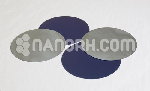
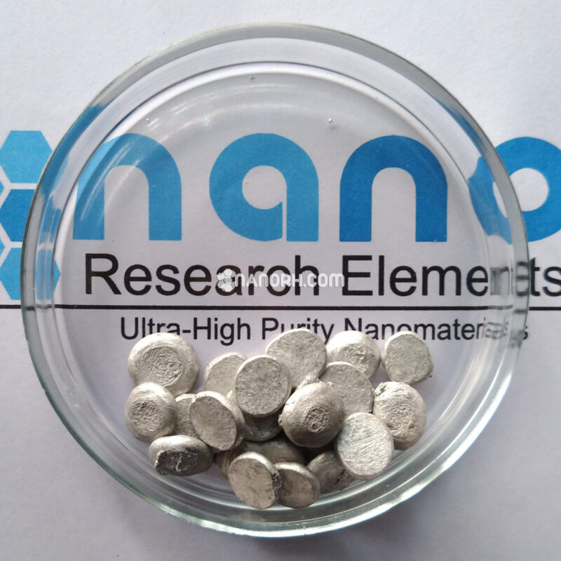
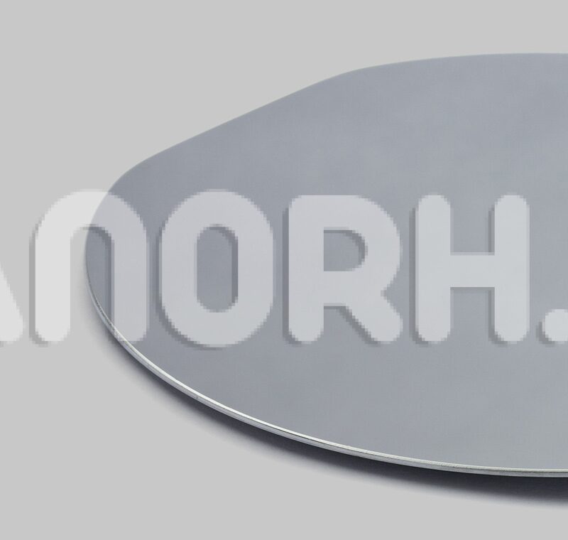
| Copper Selenide Sputtering Targets | |
| Product No | NRE-43400 |
| CAS No. | 20405-64-5 |
| Formula | Cu2Se |
| Molecular Weight | 206.063 g/mol |
| Purity | >99.9% |
| Density | 6.84 g/mL |
| Thickness | 3 mm ± 0.5mm (can be customized) |
| Diameter | 50 mm ± 1mm (can be customized) |
| Shape | Round |
| Resistivity | NA |
| Thermal Conductivity | NA |
Copper Selenide Sputtering Targets
Copper selenide (Cu₂Se) sputtering targets are used in various advanced technological applications due to their unique electrical and optical properties. Here’s a detailed overview of their primary uses.
Photovoltaic Solar Cells
Thin-Film Solar Cells: Cu₂Se is used in the production of thin-film solar cells. As an absorber layer, Cu₂Se can help in converting sunlight into electricity efficiently. The material’s strong light absorption characteristics and suitable bandgap make it a good candidate for high-performance solar cells.
High-Efficiency Devices: The efficiency of Cu₂Se-based solar cells can be comparable to or exceed other thin-film technologies, making them attractive for high-efficiency applications.
Optoelectronic Devices
Photodetectors and Light Sensors: Due to its semiconductor properties, Cu₂Se is used in optoelectronic devices such as photodetectors and light sensors. These devices can benefit from Cu₂Se’s ability to absorb light and convert it into an electrical signal.
Photodetectors: Cu₂Se is also used in infrared photodetectors, where it helps in detecting infrared radiation, which is useful for various imaging and sensing applications.
Thermoelectric Materials
Thermoelectric Devices: Cu₂Se is investigated for use in thermoelectric materials, which can convert heat into electricity. Its properties can be optimized for applications in energy generation and cooling systems, where thermoelectric effects are utilized.
Thin-Film Transistors (TFTs)
Display Technologies: Cu₂Se can be used in the fabrication of thin-film transistors, which are integral to displays such as LCDs and OLEDs. The semiconductor properties of Cu₂Se can contribute to the performance of these transistors.
Research and Development
Material Science: Cu₂Se sputtering targets are used in research to explore and develop new materials and technologies. This includes studying the effects of various processing conditions on the properties of Cu₂Se films and their potential applications in different devices.
Optical Coatings
Specialized Coatings: Cu₂Se films can be used in optical coatings where specific optical properties are required. This includes applications where unique light absorption or reflection characteristics are needed.