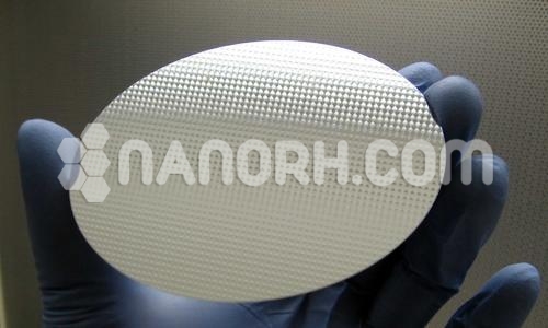
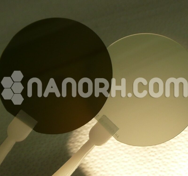
Gallium Sulfide Sputtering Targets
Gallium Sulfide Sputtering Targets
| Gallium Sulfide Sputtering Targets | |
| Product No | NRE-43423 |
| CAS No. | 12024-22-5 |
| Formula | Ga2S3 |
| Molecular Weight | 235.644 g/mol |
| Purity | >99.9% |
| Density | 3.77 g/cm3 |
| Thickness | 3 mm ± 0.5mm (can be customized) |
| Diameter | 50 mm ± 1mm (can be customized) |
| Shape | Round |
| Resistivity | NA |
| Thermal Conductivity | NA |
Gallium Sulfide Sputtering Targets
Gallium sulfide (GaS) sputtering targets are used in various applications due to their semiconductor properties and unique characteristics. Here are some key applications.
Optoelectronics
Light-Emitting Diodes (LEDs): GaS is used in the fabrication of LEDs, particularly in the green and blue regions of the spectrum.
Laser Diodes: It can be employed in laser diodes, contributing to efficient light generation.
Photodetectors
Infrared and Visible Light Sensors: GaS is utilized in photodetectors for detecting infrared and visible light, making it suitable for imaging and sensing applications.
Solar Cells
Thin-Film Photovoltaics: GaS can be used as a light-absorbing layer in thin-film solar cells, enhancing the overall efficiency of energy conversion.
Nonlinear Optical Applications
Frequency Doubling: GaS exhibits nonlinear optical properties that can be utilized in frequency conversion and other nonlinear optical devices.
2D Materials Research
Layered Semiconductor Studies: GaS is a member of the transition metal dichalcogenides (TMDs) and is of interest in research for developing new two-dimensional materials for advanced electronics.
Thin Film Transistors (TFTs)
Display Technologies: GaS can be used in the production of TFTs, improving performance in flat-panel displays and other electronic devices.
Summary
Gallium sulfide sputtering targets are versatile materials in optoelectronics, sensing technologies, and renewable energy applications. Their semiconductor properties make them valuable for a range of innovative technologies.