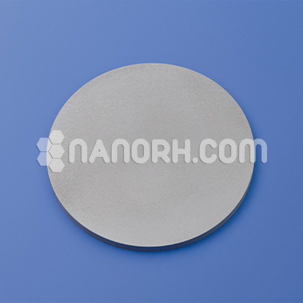
| Indium Phosphide Sputtering Targets | |
| Product No | NRE-43447 |
| CAS No. | 22398-80-7 |
| Formula | InP |
| Molecular Weight | 145.79 |
| Purity | >99.9% |
| Density | 4.81 g/cm3 |
| Thickness | 3 mm ± 0.5mm (can be customized) |
| Diameter | 50 mm ± 1mm (can be customized) |
| Shape | Round |
| Resistivity | NA |
| Thermal Conductivity | NA |
Indium Phosphide Sputtering Targets
Introduction
Indium phosphide (InP) sputtering targets are specialized materials used in the deposition of thin films for high-performance electronic and optoelectronic applications. Known for its excellent electronic and optical properties, InP is a compound semiconductor that plays a crucial role in advanced technology.
Applications:
High-Speed Electronics: InP is widely used in the fabrication of high-frequency and high-speed electronic devices, such as transistors and integrated circuits, particularly for telecommunications.
Optoelectronics: Due to its direct bandgap, InP is used in lasers, photodetectors, and light-emitting diodes (LEDs) that operate in the infrared range, making it essential for fiber optic communication systems.
Photonic Devices: InP is crucial in developing photonic integrated circuits, which are used in advanced communication technologies and signal processing.
Solar Cells: InP is also explored for use in high-efficiency multi-junction solar cells, enhancing energy conversion efficiency.
Quantum Dots: InP quantum dots are studied for their applications in displays and biological imaging due to their tunable optical properties.
Deposition Process:
Sputtering is a preferred method for depositing InP films because it allows for precise control over film thickness and composition, which is essential for achieving the desired electrical and optical characteristics in the final films.


