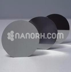
Tantalum Sputtering Target
Tantalum Sputtering Target
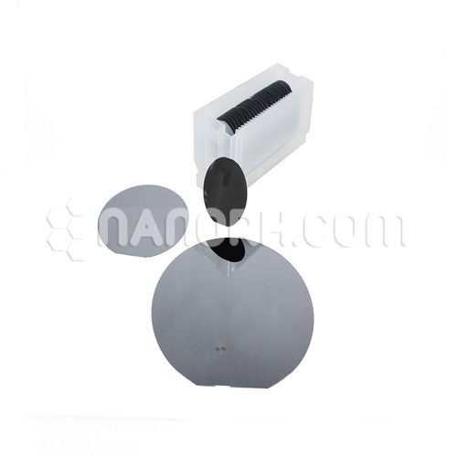
| Tantalum Sputtering Target | |
| Product No | NRE-43148-400 |
| Purity | 99.99% |
| Diameter | 400 mm |
| Thickness | 6 mm |
| Purity | 99.99% |
| With copper backing plate | |
| Purity | 99.9% |
| Diameter | 400 mm |
| Thickness | 6 mm |
| Bonded With | Indium |
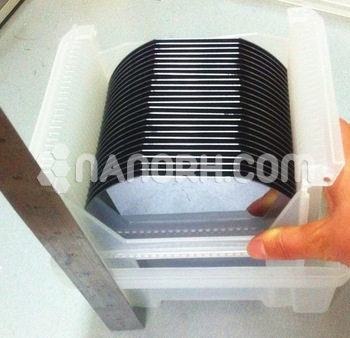
Tantalum Sputtering Target
Tantalum Sputtering Target Applications
Tantalum (Ta) sputtering targets are widely used in thin film deposition processes due to tantalum’s excellent properties: high melting point, corrosion resistance, and excellent electrical conductivity. Below are the main applications of tantalum sputtering targets:
- Semiconductor Industry
Barrier Layers in Integrated Circuits (ICs):
Tantalum and tantalum nitride (TaN) films are used as diffusion barriers between copper interconnects and silicon wafers.
Prevents copper migration into the dielectric layers.
Memory Devices:
Used in dynamic RAM (DRAM), MRAM, and flash memory for creating reliable barrier and electrode layers.
- Thin Film Resistors
Tantalum nitride thin films are used for:
Precision resistors with high thermal stability and corrosion resistance.
On-chip resistors in analog and RF circuits.
- Optical Coatings
Applied in anti-reflective and protective coatings for optical devices, lenses, and display panels.
Offers high refractive index and excellent film adhesion.
- Data Storage Devices
Used in hard disk drives (HDDs):
As part of magnetic multilayer structures.
Improves adhesion, corrosion resistance, and thermal stability of layers.
- Biomedical Applications
Thin tantalum coatings are used on medical implants due to:
Biocompatibility.
High corrosion resistance in body fluids.
- Solar Cells
Tantalum oxide (Ta₂O₅) films can serve as:
Dielectric layers in thin-film solar cells.
Transparent conductive oxide layers when doped.
- Defense and Aerospace
High-purity tantalum thin films are used in high-reliability electronics, such as:
Satellite systems.
Military communication and radar equipment.
- Display Technologies
Used in the production of TFT (Thin-Film Transistor) backplanes for LCD and OLED displays.
Acts as electrode material or adhesion layer.
If you’re using tantalum targets with copper backing plates and indium bonding, it indicates magnetron sputtering or high-temperature vacuum deposition applications, common in semiconductor foundries and advanced R&D labs.